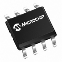
MCP1252-33X50I/MS Microchip Technology, MCP1252-33X50I/MS Datasheet - Page 9

MCP1252-33X50I/MS
Manufacturer Part Number
MCP1252-33X50I/MS
Description
IC CHRGPUMP DC/DCCONV 3.3V 8MSOP
Manufacturer
Microchip Technology
Type
Step-Down (Buck), Step-Up (Boost), Switched Capacitor (Charge Pump)r
Specifications of MCP1252-33X50I/MS
Package / Case
8-MSOP, Micro8™, 8-uMAX, 8-uSOP,
Internal Switch(s)
Yes
Synchronous Rectifier
No
Number Of Outputs
1
Voltage - Output
3.3V, 5V
Current - Output
120mA
Frequency - Switching
650kHz
Voltage - Input
2 ~ 5.5 V
Operating Temperature
-40°C ~ 85°C
Mounting Type
Surface Mount
Minimum Operating Temperature
- 40 C
Mounting Style
SMD/SMT
Function
Step Up/Step Down
Output Voltage
3.3 V or 5 V
Output Current
150 mA
Maximum Operating Temperature
+ 85 C
Lead Free Status / RoHS Status
Lead free / RoHS Compliant
Power - Output
-
Lead Free Status / Rohs Status
Lead free / RoHS Compliant
Available stocks
Company
Part Number
Manufacturer
Quantity
Price
Company:
Part Number:
MCP1252-33X50I/MS
Manufacturer:
MICROCHIP
Quantity:
12 000
Part Number:
MCP1252-33X50I/MS
Manufacturer:
MICROCHIP/微芯
Quantity:
20 000
4.0
4.1
The MCP1252 and MCP1253 family of devices employ
a switched capacitor charge pump to buck or boost an
input supply voltage (V
Referring to the Functional Block Diagram and
Figure 4-1, the devices perform conversion and regula-
tion in three phases. When the devices are not in shut-
down mode and a steady-state condition has been
reached, the three phases are continuously cycled
through. The first phase transfers charge from the input
to the flying capacitor (C
C-. This phase always occurs for half of the internal
oscillator period. During this phase, switches S
are closed.
Once the first phase is complete, all switches are
opened and the second phase (idle phase) is entered.
The device compares the internal or external feedback
voltage with an internal reference. If the feedback volt-
age is below the regulation point, the device transitions
to the third phase.
The third phase transfers energy from the flying capac-
itor to the output capacitor connected to V
load. If regulation is maintained, the device returns to
the idle phase. If the charge transfer occurs for half the
internal oscillator period, more charge is needed in the
flying capacitor and the device transitions back to the
first phase.
The regulation control is hysteretic, otherwise referred
to as a bang-bang control. The output is regulated
around a fixed reference with some hysteresis. As a
result, typically 50 mV of peak-to-peak ripple will be
observed at the output independent of load current.
The frequency of the output ripple, however, will be
influenced heavily by the load current and output
capacitance. The maximum frequency that will be
observed is equal to the internal oscillator frequency.
The devices automatically transition between buck or
boost operation. This provides a low-cost, compact and
simple solution for step-down/step-up DC/DC conver-
sion. This is especially true for battery-operated appli-
cations that require a fixed output above or below the
input.
2002 Microchip Technology Inc.
DEVICE OVERVIEW
Theory of Operation
IN
FLY
) to a regulated output voltage.
) connected to pins C+ and
OUT
1
and the
and S
2
FIGURE 4-1:
No
No
Yes
PHASE 3:
Charge Transfer
From C
PHASE 2:
Idle State
PHASE 1:
Charge Transfer
From V
t
t
3
1
V
V
Flow Algorithm.
FB
= 2F
FB
= 2F
START
MCP1252/3
FLY
> V
> V
IN
OSC
OSC
1
1
Yes
No
No
to C
to C
REF
REF
FLY
OUT
Yes
Yes
DS21752A-page 9


