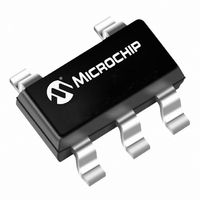
TCM829ECT713 Microchip Technology, TCM829ECT713 Datasheet - Page 3

TCM829ECT713
Manufacturer Part Number
TCM829ECT713
Description
IC CHARGE PUMP CONV SOT23A-5
Manufacturer
Microchip Technology
Type
Switched Capacitor (Charge Pump), Doubler, Invertingr
Specifications of TCM829ECT713
Internal Switch(s)
Yes
Synchronous Rectifier
No
Number Of Outputs
1
Voltage - Output
-1.5 ~ -5.5 V, ±3 ~ ±11 V
Current - Output
25mA
Frequency - Switching
35kHz
Voltage - Input
1.5 ~ 5.5 V
Operating Temperature
-40°C ~ 85°C
Mounting Type
Surface Mount
Package / Case
SOT-23-5, SC-74A, SOT-25
Power - Output
240mW
Primary Input Voltage
5.5V
No. Of Outputs
1
Output Current
25mA
No. Of Pins
5
Operating Temperature Range
-40°C To +85°C
Peak Reflow Compatible (260 C)
Yes
Switching Frequency Max
35kHz
Function
Inverting, Step Up
Output Voltage
- 1.5 V to - 5.5 V, 3 V to 11 V
Maximum Operating Temperature
85 C
Minimum Operating Temperature
- 40 C
Mounting Style
SMD/SMT
Lead Free Status / RoHS Status
Lead free / RoHS Compliant
Lead Free Status / RoHS Status
Lead free / RoHS Compliant, Lead free / RoHS Compliant
Other names
158-2032-2
158-2032-2
TCM829ECT713RTR
TCM829ECT713RTR
TCM829ECT713TR
158-2032-2
TCM829ECT713RTR
TCM829ECT713RTR
TCM829ECT713TR
Available stocks
Company
Part Number
Manufacturer
Quantity
Price
Part Number:
TCM829ECT713
Manufacturer:
MICROCHIP/微芯
Quantity:
20 000
Company:
Part Number:
TCM829ECT713-GVAO
Manufacturer:
TOSH
Quantity:
5 082
Switched Capacitor
Voltage Converters
© 2001 Microchip Technology Inc.
DETAILED DESCRIPTION
voltage applied to the V
phase operation (Figure 1). During the first phase, switches
S2 and S4 are open and S1 and S3 are closed. During this
time, C1 charges to the voltage on V
supplied from C2. During the second phase, S2 and S4 are
closed, and S1 and S3 are open. This action connects C1
across C2, restoring charge to C2.
APPLICATIONS INFORMATION
Output Voltage Considerations
not provide regulation . The output voltage will droop in a
linear manner with respect to load current. The value of this
equivalent output resistance is approximately 25 nominal
at +25 C and V
loads, and droops according to the equation below:
Charge Pump Efficiency
affected by four factors:
The TCM828/829 charge pump converters invert the
The TCM828/829 perform voltage conversion but do
The overall power efficiency of the charge pump is
(1) Losses from power consumed by the internal oscil-
(2) I
(3) Charge pump capacitor losses due to effective
IN
V
lator, switch drive, etc. (which vary with input volt-
age, temperature and oscillator frequency).
switches on-board the charge pump.
series resistance (ESR).
Figure 1. Ideal Switched Capacitor Charge Pump
2
DROOP
R losses due to the on-resistance of the MOSFET
V
OUT
S3
S1
IN
= – (V
= I
= +5V. V
C1
OUT
DS21488A
IN
IN
x R
S4
– V
pin. Conversion consists of a two-
OUT
S2
OUT
DROOP
is approximately – 5V at light
)
IN
C2
TCM828/829
and load current is
V
OUT
= – (V
IN
)
3
and (4) above. These losses are given by Equation 1.
output resistance of an ideal switched capacitor circuit
(Figures 2a, 2b).
are also shown in Equation 2. The output voltage ripple is
given by Equation 3.
(4) Losses that occur during charge transfer (from the
Most of the conversion losses are due to factors (2), (3)
The 1/(f
The losses in the circuit due to factor (4) above
P
V
P
LOSS (4)
RIPPLE
LOSS (2, 3, 4)
I
OUT
V
commutation capacitor to the output capacitor)
when a voltage difference between the two capaci-
tors exists.
V
+
+
R
2
Figure 2a. Ideal Switched Capacitor Model
EQUIV =
=
OSC
x
=
Figure 2b. Equivalent Output Resistance
C1
[
(f
[
R
(f
OSC
)(C1) term in Equation 1 is the effective
(0.5)(C1)(V
– 2V
EQUIV
OSC
I
f
= I
OUT
)(C2)
f x C1
1
OUT
) C1
OUT
1
2
V
Equation 1.
Equation 2.
+2(I
Equation 3.
x R
+8R
RIPPLE
IN
2
OUT
C2
OUT
– V
SWITCH
C2
)
OUT
)(ESR
]
2
x f
+ 4ESR
) + (0.5)(C2)(V
OSC
C2
R
L
)
R
V
L
OUT
C1
V
TCM828/829-4 5/22/00
OUT
TCM828
TCM829
+ ESR
RIPPLE
C2
]
2


