MAX5089ATE+ Maxim Integrated Products, MAX5089ATE+ Datasheet - Page 14
MAX5089ATE+
Manufacturer Part Number
MAX5089ATE+
Description
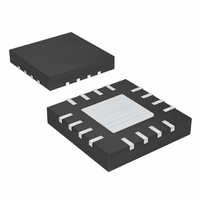
IC DC-DC CONV BUCK 16TQFN
Manufacturer
Maxim Integrated Products
Type
Step-Down (Buck)r
Datasheet
1.MAX5089ATE.pdf
(24 pages)
Specifications of MAX5089ATE+
Internal Switch(s)
Yes
Synchronous Rectifier
Yes
Number Of Outputs
1
Voltage - Output
0.6 ~ 20 V
Current - Output
2A
Frequency - Switching
200kHz ~ 2.2MHz
Voltage - Input
4.5 ~ 23 V
Operating Temperature
-40°C ~ 125°C
Mounting Type
Surface Mount
Package / Case
16-TQFN Exposed Pad
Power - Output
2.67W
Lead Free Status / RoHS Status
Lead free / RoHS Compliant


The MAX5088/MAX5089 can operate with input sup-
plies ranging from 4.5V to 5.5V or 5.5V to 23V. The
input voltage range (V+) can be constrained to a mini-
mum by the duty-cycle limitations and to a maximum by
the on-time limitation. The minimum input voltage is
determined by:
D
V
that includes the diode’s forward voltage drop (or the
drop across the synchronous rectifier MOSFET), and
the drops across the series resistance of the inductor
and PC board traces. V
inductors charging path, which includes the drop
across the internal power MOSFET, and the drops
across the series resistance of the inductor and PC
board traces.
The maximum input voltage can be determined by:
where t
quency.
For 0.6V or greater output voltages, connect a resistive
divider from V
SGND resistor (R2) between 1kΩ and 10kΩ and calcu-
late the resistor from OUT to FB (R1) by the following
equation:
where V
For designs that use a Type III compensation scheme,
first calculate R1 for stability requirements (see the
Compensation section) then choose R2 so that:
See Figure 4.
Three key inductor parameters must be specified for
operation with the MAX5088/MAX5089: inductance
2.2MHz, 2A Buck Converters with an
Integrated High-Side Switch
14
DROP1
MAX
______________________________________________________________________________________
V
IN MIN
is the maximum duty cycle of 87.5% (typ).
ON_MIN
FB
is the total drop in the inductor discharge path
_
= 0.6V, see Figure 3.
=
OUT
V
= 100ns and f
V
IN MAX
OUT
R
_
1
R
to FB to SGND. Select the FB to
=
D
2
R
+
MAX
=
2
V
Effective Input Voltage Range
=
V
DROP2
DROP
×
R
OUT
t
1
ON MIN
Setting the Output Voltage
V
V
×
OUT
FB
1
_
−
V
SW
V
+
OUT
V
is the total drop in the
FB
FB
V
−
DROP
is the switching fre-
1
×
Inductor Selection
f
SW
2
−
V
DROP
1
value (L), peak inductor current (I
saturation current (I
tance is a function of operating frequency, input-to-out-
put voltage differential, and the peak-to-peak inductor
current (∆I
value, while a lower ∆I
value. A lower inductor value minimizes size and cost,
improves large-signal and transient response, but
reduces efficiency due to higher peak currents and
higher peak-to-peak output voltage ripple for the same
output capacitor. On the other hand, higher inductance
increases efficiency by reducing the ripple current.
Resistive losses due to extra wire turns can exceed the
benefit gained from lower ripple current levels especial-
ly when the inductance is increased without also allow-
ing for larger inductor dimensions. A good compromise
is to choose ∆I
Use the following equation to calculate the inductance:
V
optimum for typical conditions. The switching frequency
is set by R
section). The peak-to-peak inductor current, which
reflects the peak-to-peak output ripple, is worse at the
maximum input voltage. See the Output Capacitor
Selection section to verify that the worst-case output rip-
ple is acceptable. The inductor saturation current is also
important to avoid runaway current during continuous
output short-circuit. At high input-to-output differential,
and high switching frequency, the on-time drops to the
order of 100ns. Though the MAX5088/MAX5089 can
control the on-time as low as 100ns, the internal current-
limit circuit may not detect the overcurrent within this
time. In that case, the output current during the fault
may exceed the current limit specified in the EC table.
The overtemperature shutdown protects the
MAX5088/MAX5089 against the output short-circuit
fault. However, the output current may reach 5.5A.
Choose an inductor with a saturation current of greater
than 5.5A when the minimum on-time for a given fre-
quency and duty cycle is less than 200ns.
The discontinuous input current of the buck converter
causes large input ripple current. The switching frequen-
cy, peak inductor current, and the allowable peak-to-
peak input voltage ripple dictate the input capacitance
requirement. Increasing the switching frequency or the
inductor value lowers the peak-to-average current ratio
yielding a lower input capacitance requirement.
IN
and V
OSC
P-P
OUT
). Higher ∆I
P-P
(see the Setting the Switching Frequency
are typical values so that efficiency is
L
equal to 30% of the full load current.
=
SAT
V
V
OUT IN
I
N
). The minimum required induc-
P-P
×
P-P
(V
f
SW
requires a higher inductor
allows for a lower inductor
−
×
V
∆
OUT
I
P P
PEAK
−
)
Input Capacitors
), and inductor
Related parts for MAX5089ATE+
Image
Part Number
Description
Manufacturer
Datasheet
Request
R

Part Number:
Description:
2.2MHz - 2A Buck Converters with an Integrated High-Side Switch
Manufacturer:
Maxim Integrated Products
Datasheet:

Part Number:
Description:
Voltage-Output, 12-Bit DACs with Internal Reference
Manufacturer:
MAXIM [Maxim Integrated Products]
Datasheet:
Part Number:
Description:
MAX7528KCWPMaxim Integrated Products [CMOS Dual 8-Bit Buffered Multiplying DACs]
Manufacturer:
Maxim Integrated Products
Datasheet:
Part Number:
Description:
Single +5V, fully integrated, 1.25Gbps laser diode driver.
Manufacturer:
Maxim Integrated Products
Datasheet:
Part Number:
Description:
Single +5V, fully integrated, 155Mbps laser diode driver.
Manufacturer:
Maxim Integrated Products
Datasheet:
Part Number:
Description:
VRD11/VRD10, K8 Rev F 2/3/4-Phase PWM Controllers with Integrated Dual MOSFET Drivers
Manufacturer:
Maxim Integrated Products
Datasheet:
Part Number:
Description:
Highly Integrated Level 2 SMBus Battery Chargers
Manufacturer:
Maxim Integrated Products
Datasheet:
Part Number:
Description:
Current Monitor and Accumulator with Integrated Sense Resistor; ; Temperature Range: -40°C to +85°C
Manufacturer:
Maxim Integrated Products
Part Number:
Description:
TSSOP 14/A°/RS-485 Transceivers with Integrated 100O/120O Termination Resis
Manufacturer:
Maxim Integrated Products
Part Number:
Description:
TSSOP 14/A°/RS-485 Transceivers with Integrated 100O/120O Termination Resis
Manufacturer:
Maxim Integrated Products
Part Number:
Description:
QFN 16/A°/AC-DC and DC-DC Peak-Current-Mode Converters with Integrated Step
Manufacturer:
Maxim Integrated Products
Part Number:
Description:
TDFN/A/65V, 1A, 600KHZ, SYNCHRONOUS STEP-DOWN REGULATOR WITH INTEGRATED SWI
Manufacturer:
Maxim Integrated Products
Part Number:
Description:
Integrated Temperature Controller f
Manufacturer:
Maxim Integrated Products
Part Number:
Description:
SOT23-6/I°/45MHz to 650MHz, Integrated IF VCOs with Differential Output
Manufacturer:
Maxim Integrated Products
Part Number:
Description:
SOT23-6/I°/45MHz to 650MHz, Integrated IF VCOs with Differential Output
Manufacturer:
Maxim Integrated Products