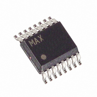
MAX8543EEE+ Maxim Integrated Products, MAX8543EEE+ Datasheet - Page 21

MAX8543EEE+
Manufacturer Part Number
MAX8543EEE+
Description
IC CNTRLR STEP DOWN 16-QSOP
Manufacturer
Maxim Integrated Products
Type
Step-Down (Buck)r
Datasheet
1.MAX8543EEE.pdf
(27 pages)
Specifications of MAX8543EEE+
Internal Switch(s)
No
Synchronous Rectifier
No
Number Of Outputs
1
Voltage - Output
0.8 ~ 11 V
Current - Output
25A
Frequency - Switching
200kHz ~ 1MHz
Voltage - Input
3 ~ 13.2 V
Operating Temperature
-40°C ~ 85°C
Mounting Type
Surface Mount
Package / Case
16-QSOP
Power - Output
667mW
Output Voltage
0.8 V to 11.88 V
Output Current
25000 mA
Mounting Style
SMD/SMT
Switching Frequency
200 KHz to 1000 KHz
Maximum Operating Temperature
+ 85 C
Minimum Operating Temperature
- 40 C
Synchronous Pin
Yes
Topology
Buck
Lead Free Status / RoHS Status
Lead free / RoHS Compliant
The MAX8543/MAX8544 drive two or four external,
logic-level, n-channel MOSFETs as the circuit switch
elements. The key selection parameters are:
1) On-resistance (R
2) Maximum drain-to-source voltage (V
3) Gate charges (Q
For a 3.3V input application, choose a MOSFET with a
rated R
choose the MOSFETs with rated R
For a good compromise between efficiency and cost,
choose the high-side MOSFET (N1, N2) that has conduc-
tion losses equal to the switching loss at nominal input
voltage and output current. The selected low-side
MOSFET (N3, N4) must have an R
current-limit-setting condition above. Ensure that the low-
side MOSFET does not spuriously turn on due to dV/dt
caused by the high-side MOSFET turning on as this
would result in shoot-through current and degrade the
efficiency. MOSFETs with a lower Q
higher immunity to dV/dt. For high-current applications, it
is often preferable to parallel two MOSFETs rather than to
use a single large MOSFET.
For proper thermal-management design, the power dis-
sipation must be calculated at the desired maximum
operating junction temperature, maximum output current,
and worst-case input voltage (for the low-side MOSFET,
worst case is at V
could be either at V
and low-side MOSFETs have different loss components
due to the circuit operation. The low-side MOSFET oper-
ates as a zero-voltage switch; therefore, major losses
are the channel-conduction loss (P
diode conduction loss (P
Use R
where V
the dead time between high-side and low-side switching
transitions, and f
be at least 20% higher than the input supply rail at
the high-side MOSFET’s drain.
DS(ON)
P
DS(ON)
LSCC
P
F
Lossless Sensing, Synchronization, and OVP
Step-Down Controllers with Prebias Startup,
LSDC
is the body-diode forward-voltage drop, t
at T
=
at V
=
⎛
⎜
⎝
S
1
2
J(MAX)
−
is the switching frequency.
IN(MAX)
GS
______________________________________________________________________________________
×
V
G
IN(MAX)
DS(ON)
OUT
V
I
, Q
= 2.5V. For a 5V input application,
IN
LOAD
:
GD
LSDC
; for the high-side MOSFET, it
⎞
⎟ ×
⎠
, Q
): the lower, the better.
or V
×
):
GS
I
2
LOAD
V
MOSFET Selection
F
): the lower, the better.
DS(ON)
IN(MIN)
DS(ON)
LSCC
×
GD
×
t
DT
/ Q
). The high-side
R
) and the body-
that satisfies the
at V
DS ON
×
DSS
GS
(
f
GS
S
ratio have
): should
)
≤ 4.5V.
DT
is
The high-side MOSFET operates as a duty-cycle control
switch and has the following major losses: the channel-
conduction loss (P
loss (P
MOSFET does not have body-diode conduction loss
because the diode never conducts current:
Use R
where I
capability determined by:
where R
on-resistance (1Ω, typ) and R
resistance of the MOSFET (≈0.5Ω to 3Ω):
where V
In addition to the losses above, allow about 20% more for
additional losses due to MOSFET output capacitances
and low-side MOSFET body-diode reverse-recovery
charge dissipated in the high-side MOSFET, but it is not
well defined in the MOSFET data sheet. Refer to the
MOSFET data sheet for thermal resistance specifications
to calculate the PC board area needed to maintain the
desired maximum operating junction temperature with the
above calculated power dissipations.
To reduce EMI caused by switching noise, add a 0.1µF
ceramic capacitor from the high-side switch drain to
the low-side switch source or add resistors in series
with DH and DL to slow down the switching transitions.
However, adding series resistors increases the power
dissipation of the MOSFET, so be sure this does not
overheat the MOSFET.
P
HSDR
P
DS(ON)
HSSW
HSSW
GATE
GS
DS(ON)(HS)
=
P
HSCC
Q
≈ V
), and the drive loss (P
G
I
GATE
=
at T
is the average DH-driver output current
VL.
V
×
IN
=
J(MAX)
V
V
≅
HSCC
GS
×
OUT
V
IN
is the high-side MOSFET driver’s
R
I
LOAD
DS ON HS
×
:
), the VI overlapping switching
(
×
f
0 5 .
S
I
2
LOAD
)(
×
×
×
GATE
R
Q
)
V
GATE
+
GS
VL
I
HSDR
×
R
GATE
is the internal gate
GATE
+
R
Q
R
DS ON
+
). The high-side
GD
GATE
R
(
DS ON HS
×
(
)
f
S
)(
)
21


