LM5085SDE/NOPB National Semiconductor, LM5085SDE/NOPB Datasheet - Page 18

LM5085SDE/NOPB
Manufacturer Part Number
LM5085SDE/NOPB
Description
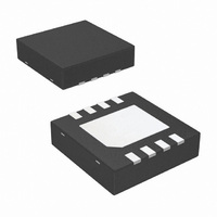
IC BUCK ADJ 8LLP
Manufacturer
National Semiconductor
Series
PowerWise®r
Type
Step-Down (Buck)r
Datasheet
1.LM5085MYENOPB.pdf
(22 pages)
Specifications of LM5085SDE/NOPB
Design Resources
LM(2)5085 Quick Start Calculator
Internal Switch(s)
No
Synchronous Rectifier
No
Number Of Outputs
1
Voltage - Output
1.25 ~ 75 V
Frequency - Switching
Up to 1MHz
Voltage - Input
4.5 ~ 75 V
Operating Temperature
-40°C ~ 125°C
Mounting Type
Surface Mount
Package / Case
8-LLP
Lead Free Status / RoHS Status
Lead free / RoHS Compliant
Current - Output
-
Power - Output
-
Other names
LM5085SDETR
Available stocks
Company
Part Number
Manufacturer
Quantity
Price
Company:
Part Number:
LM5085SDE/NOPB
Manufacturer:
NS
Quantity:
70
Part Number:
LM5085SDE/NOPB
Manufacturer:
TI/德州仪器
Quantity:
20 000
www.national.com
Alternate Output Ripple
Configurations
The minimum ripple configuration, employing C1, C2, and R3
in figure 4, results in a low ripple amplitude at V
mined mainly by the characteristics of the output capacitor
and the ripple current in L1. This configuration allows multiple
ceramic capacitors to be used for V
is provided to several places on the PC board. However, if a
slightly higher level of ripple at V
plication, and distributed capacitance is not used, the ripple
required for the FB comparator pin can be generated with
fewer external components using the circuits shown below.
a) Reduced ripple configuration: In Figure 9, R3, C1 and
C2 are removed (compared to Figure 4). A low value resistor
(R4) is added in series with C
added across R
inductor’s ripple current flowing through R4, and that ripple
voltage is passed to the FB pin via Cff. The ripple at V
b) Lowest cost configuration: This configuration, shown in
Figure 10, is the same as Figure 9 except Cff is removed.
Since the ripple voltage at V
R
FB1
, the minimum ripple required at V
V
RIP(min)
FB2
= 25 mV x (R
. Ripple is generated at V
OUT
OUT
OUT
FB2
FIGURE 10. Lowest Cost Ripple Generating Configuration
is attenuated by R
, and a capacitor (Cff) is
OUT
+ R
is acceptable in the ap-
OUT
FB1
if the output voltage
FIGURE 9. Reduced Ripple Configuration
is equal to:
)/R
FB1
OUT
OUT
OUT
FB2
by the
deter-
and
can
18
be set as low as 25 mVp-p since it is not attenuated by R
and R
where I
minimum input voltage. The minimum value for Cff is deter-
mined from:
where t
imum VIN. The next larger standard value capacitor should
be used for Cff.
The minimum value for R4 is calculated from:
where I
minimum input voltage.
FB1
OR(min)
ON(max)
OR(min)
. The minimum value for R4 is calculated from:
is the minimum ripple current, which occurs at
is the minimum ripple current, which occurs at
is the maximum on-time, which occurs at min-
30057749
30057751
FB2


