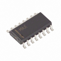
MAX798ESE+ Maxim Integrated Products, MAX798ESE+ Datasheet - Page 8

MAX798ESE+
Manufacturer Part Number
MAX798ESE+
Description
IC CNTRLR STEP DOWN 16-SOIC
Manufacturer
Maxim Integrated Products
Type
Step-Down (Buck)r
Datasheet
1.MAX798ESE.pdf
(12 pages)
Specifications of MAX798ESE+
Internal Switch(s)
No
Synchronous Rectifier
Yes
Number Of Outputs
1
Voltage - Output
1.6 ~ 6 V
Current - Output
10A
Frequency - Switching
150kHz, 300kHz
Voltage - Input
4.5 ~ 30 V
Operating Temperature
-40°C ~ 85°C
Mounting Type
Surface Mount
Package / Case
16-SOIC (3.9mm Width)
Power - Output
696mW
Lead Free Status / RoHS Status
Lead free / RoHS Compliant
These internal IC blocks aren’t powered directly from
the battery. Instead, a +5V linear regulator steps down
the battery voltage to supply both the IC internal rail (VL
pin) as well as the gate drivers. The synchronous-
switch gate driver is directly powered from +5V VL,
while the high-side-switch gate driver is indirectly pow-
ered from VL via an external diode-capacitor boost cir-
cuit. An automatic bootstrap circuit turns off the +5V
linear regulator and powers the IC from its output volt-
age if the output is above 4.5V.
The heart of the current-mode PWM controller is a multi-
input open-loop comparator that sums three
signals: output voltage error signal with respect to the
reference voltage, current-sense signal, and slope
compensation ramp (Figure 3). The PWM controller is
a direct summing type, lacking a traditional error
amplifier and the phase shift associated with it. This
direct-summing configuration approaches the ideal of
cycle-by-cycle control over the output voltage.
For more comprehensive information on the MAX798
internal blocks, please refer to the MAX796/MAX797/
MAX799 data sheet.
If the circuit’s output voltage is greater than the VL/CSL
switchover voltage, the IC automatically bootstraps and
runs off its output. Running from the high-efficiency out-
put rather than the VL linear regulator is particularly
desirable if the input voltage is high. If the output is
not greater than the VL/CSL switchover threshold,
efficiency can be improved by powering VL from
another efficient system supply (Figure 4).
VL can be connected directly to a +5V supply, provid-
ed its maximum excursions are within a 4.5V to 6V
range and the main output voltage’s maximum is less
than 4.2V. If the circuit’s output voltage is greater than
4.2V, the IC can activate its internal bootstrap switch
and connect the circuit output to VL.
High-Accuracy Step-Down Controller
with Synchronous Rectifier for CPU Power
8
__________Applications Information
_______________________________________________________________________________________
Powering VL from a +5V Supply
PWM Controller Block
The output voltage is set by an external resistor divider
between the output voltage and GND, with the midpoint
connected to FB (Figure 5). The output voltage can be
adjusted from 1.6V to 6V, according to the formula in
Figure 5. Recommended R2 values range from 5k
100k . For best noise immunity, place R1 and R2 close
to FB. For a 1.6V output, connect the output voltage
directly to FB.
Remote sensing of the output voltage is easily achieved
by connecting the top of R1 and, if desired, the bottom
of R2, to the remote sense point.
The MAX798 is designed to deliver a more accurate
output voltage than the MAX797. A major source of the
MAX797’s output error is the decrease in output voltage
with increasing load. This error is greatly reduced in the
MAX798 by increasing the gain of the voltage-sense
signal relative to the current-sense signal. As a result of
this increased gain, the MAX798 is slightly more noise
sensitive than the MAX797, and requires some small
compensation components as well. On the other hand,
output capacitor ESR requirements can be greatly
relaxed compared to the MAX797, with the limiting fac-
tor being the maximum total output voltage ripple that
the application can tolerate.
To control noise problems, place the bypass capacitors
on REF, VL, and V+ as close as possible to the IC, and
use a 10Ω series resistor (R3, Figure 1) on V+ to form a
small lowpass filter. Feed-forward components (R4, C3,
and C5) are chosen for stable switching at 150kHz with
the components shown. For 300kHz switching and a
4.7µH inductor, use R4 = 470k Ω and C5 = 220pF.
Keep the components that connect to FB (R4, C5, R1,
R2) close to the IC’s FB pin.
With the exception of the items previously mentioned,
follow the design procedure for the MAX797. The
MAX796/MAX797/MAX799 data sheet contains all nec-
essary information on component values, component
selection, layout, and additional applications.
Adjusting the Output Voltage
Compensation Components
Design Procedure
Bypassing and
to


