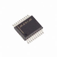
MAX1623EAP+ Maxim Integrated Products, MAX1623EAP+ Datasheet - Page 10

MAX1623EAP+
Manufacturer Part Number
MAX1623EAP+
Description
IC REG LV SYNC 3A STEPDWN 20SSOP
Manufacturer
Maxim Integrated Products
Type
Step-Down (Buck)r
Datasheet
1.MAX1623EAP.pdf
(12 pages)
Specifications of MAX1623EAP+
Internal Switch(s)
Yes
Synchronous Rectifier
Yes
Number Of Outputs
1
Voltage - Output
1.1 ~ 3.8 V
Current - Output
3A
Frequency - Switching
Up to 350kHz
Voltage - Input
4.5 ~ 5.5 V
Operating Temperature
-40°C ~ 85°C
Mounting Type
Surface Mount
Package / Case
20-SSOP
Power - Output
1.3W
Output Voltage
1.1 V to 3.8 V
Input Voltage
4.5 V to 5.5 V
Supply Current
400 uA
Switching Frequency
350 KHz
Maximum Operating Temperature
+ 85 C
Minimum Operating Temperature
- 40 C
Lead Free Status / RoHS Status
Lead free / RoHS Compliant
flow. A copper area of 0.4in
tance of 60°C/W.
Airflow over the IC can significantly reduce θ
The MAX1623’s power dissipation consists mostly of con-
duction losses in the two internal power switches. Power
dissipation due to supply current in the control section
and average current used to charge and discharge the
gate capacitance of the two power switches is less than
30mW at 300kHz. This number is reduced when switch-
ing frequency is reduced as the part enters Idle Mode.
Combined conduction loss in the two power switches is
calculated by:
where R
The θ
culated by:
where:
T
T
The inductor value can be adjusted to optimize the
design for size, cost, and efficiency. Three key inductor
parameters must be specified: inductance value (L),
peak current (I
lowing equation includes a constant, denoted as LIR,
which is the ratio of inductor peak-to-peak AC current
to DC load current. A higher value of LIR allows smaller
inductance, but results in higher losses and ripple. A
good compromise between size and losses is found at
a 30% ripple current to load current ratio (LIR = 0.3),
which corresponds to a peak inductor current 1.15
times the DC load current:
where:
f = switching frequency
I
LIR = ratio of AC to DC inductor current, typically
3A, Low-Voltage, Step-Down Regulator with
Synchronous Rectification and Internal Switches
10 _______________________________________________________________________________________
OUT
J(MAX)
A(MAX)
= maximum DC load current
JA
0.3
= maximum ambient temperature expected
ON
= maximum allowed junction temperature
required to deliver this amount of power is cal-
L
= 100mΩ (max).
θ
=
JA
PEAK
Applications Information
V
IN(MAX)
= (T
V
P
OUT IN(MAX)
D
), and DC resistance (R
J(MAX)
= I
(V
LOAD 2
×
f
– T
×
2
A(MAX)
(R
(I
showed thermal resis-
Power Dissipation
OUT
−
ON
V
OUT
)
) (LIR)
) / P
)
Inductor L1
D
DC
JA
). The fol-
.
The peak inductor current at full load is 1.15 x I
the above equation is used; otherwise, the peak current
can be calculated by:
The inductor’s DC resistance is a key parameter for effi-
ciency and must be minimized, preferably to less than
25mΩ at I
inductor.
Use a low-ESR input capacitor according to the input
ripple-current requirements and voltage rating.
In addition to C1, place a 10µF ceramic bypass capacitor
from the power input (pin 2, 4, 6) to power ground (pin
15, 17, 19) within 5mm of the IC.
The output filter capacitor determines the output volt-
age ripple and output load-transient response, as well
as the loop’s stability.
The output ripple in continuous-conduction mode is:
where f is the switching frequency.
Table 2. Suggested Values (V
I
V
O
OUT(RPL)
= 3A, f = 300kHz)
V
I
(V)
3.3
2.5
1.8
1.5
1.1
RIPPLE
OUT
I
PEAK
OUT
=
I
OUT(MAX)
=
=
= 3A. To reduce EMI, use a shielded
I
I
LOAD
OUT
T
1.10
1.67
2.16
2.38
2.68
(µs)
OFF
+
×
V
2
LIR ESR
Input and Output Filter
OUT IN(MAX)
V
×
OUT
f
Capacitors (C1, C2)
(V
×
(
R
C2
V
L
(k
120
180
240
260
280
TOFF
IN
V
Ω
IN
×
+
)
−
IN
V
IN(MAX)
2
−
V
π
V
= 5V,
OUT
OUT
×
1
f
)
)
×
(µH)
4.7
4.7
4.7
3.9
3.3
L
OUT
C2
if


