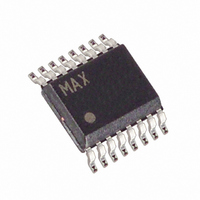
MAX8505EEE+ Maxim Integrated Products, MAX8505EEE+ Datasheet - Page 9

MAX8505EEE+
Manufacturer Part Number
MAX8505EEE+
Description
IC REG STP DWN 3A 16-QSOP
Manufacturer
Maxim Integrated Products
Type
Step-Down (Buck)r
Datasheet
1.MAX8505EEE.pdf
(15 pages)
Specifications of MAX8505EEE+
Internal Switch(s)
Yes
Synchronous Rectifier
Yes
Number Of Outputs
1
Voltage - Output
0.8 ~ 4.68 V
Current - Output
3A
Frequency - Switching
500kHz, 1MHz
Voltage - Input
2.6 ~ 5.5 V
Operating Temperature
-40°C ~ 85°C
Mounting Type
Surface Mount
Package / Case
16-QSOP
Power - Output
1W
Input Voltage
2.6 V to 5.5 V
Supply Current
6 mA
Maximum Operating Temperature
+ 85 C
Minimum Operating Temperature
- 40 C
Lead Free Status / RoHS Status
Lead free / RoHS Compliant
The MAX8505 is a high-efficiency synchronous buck
regulator capable of delivering up to 3A of output
current. It operates in PWM mode at a high fixed
frequency of 500kHz or 1MHz, thereby reducing
external component size. The MAX8505 operates from
a 2.6V to 5.5V input voltage and can produce an output
voltage from 0.8V to 0.85
The MAX8505 step-down converter uses a PWM
current-mode control scheme. An open-loop comparator
compares the voltage-feedback error signal against the
sum of the amplified current-sense signal and the slope
compensation ramp. At each rising edge of the internal
clock, the internal high-side MOSFET turns on until the
PWM comparator trips. During this on-time, current ramps
up through the inductor, sourcing current to the output
and storing energy in the inductor. The current-mode
feedback system regulates the peak inductor current as a
function of the output-voltage error signal. Since the aver-
age inductor current is nearly the same as the peak
inductor current, the circuit acts as a switch-mode
transconductance amplifier. To preserve inner-loop
stability and eliminate inductor staircasing, a slope-
1, 3, 14, 16
13, 15
PIN
2, 4
10
11
12
5
6
7
8
9
NAME
COMP
PGND
GND
POK
BST
V
CTL
REF
LX
FB
IN
CC
_______________________________________________________________________________________
3A, 1MHz, 1% Accurate, Internal Switch
Controller Block Function
Detailed Description
Inductor Connection. Connect an inductor between these pins and the regulator output. All LX pins must
be connected together externally. Connect a 3300pF ceramic capacitor from LX to PGND.
Power-Supply Inputs. Ranges from 2.6V to 5.5V. Bypass with two ceramic 22µF capacitors to GND. All IN
pins must be connected together externally.
Bootstrapped Voltage Input. High-side driver supply pin. Bypass to LX with a 0.1µF capacitor. Charged
from IN with an external Schottky diode.
Supply Voltage and Gate-Drive Supply for Low-Side Driver. Decouple with a 10Ω resistor and bypass to
GND with 0.1µF.
Power-OK Output. Open-drain output of a window comparator that pulls POK low when the FB pin is
outside the 0.8V ±12% range.
Output Control. When at GND, the regulator is off. When at V
500kHz application, raise the pin to 2/3 V
Regulator Loop Compensation. Connect a series RC network to GND. This pin is pulled to GND when the
output is shut down, or in UVLO or thermal shutdown.
Feedback Input. This pin regulates to 0.8V. Use an external resistive-divider from the output to set the
output voltage.
Place a capacitor at this pin to set the soft-start time. This pin goes to 0V when the part is shut down.
Ground
Power Ground. Connect this pin to GND at a single point.
Step-Down Regulator with Power-OK
V
IN
.
CC
compensation ramp is summed into the main PWM com-
parator. During the second half of the cycle, the internal
high-side N-channel MOSFET turns off, and the internal
low-side N-channel MOSFET turns on. The inductor
releases the stored energy as its current ramps down
while still providing current to the output. The output
capacitor stores charge when the inductor current
exceeds the load current, and discharges when the
inductor current is lower, smoothing the voltage across
the load. Under overload conditions, when the inductor
current exceeds the current limit (see the Current Limit
section), the high-side MOSFET does not turn on at the
rising edge of the clock and the low-side MOSFET
remains on to let the inductor current ramp down.
An internal current-sense amplifier produces a current
signal proportional to the voltage generated by the high-
side MOSFET on-resistance and the inductor current
(R
the internal slope-compensation signal are summed
together into the comparator’s inverting input. The PWM
comparator turns off the internal high-side MOSFET
when this sum exceeds the feedback voltage from the
voltage-error amplifier.
.
DS(ON)
FUNCTION
I
LX
). The amplified current-sense signal and
CC
, the regulator is operating at 1MHz. For a
Pin Description
Current Sense
9


