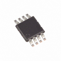
MAX1606EUA+ Maxim Integrated Products, MAX1606EUA+ Datasheet - Page 9

MAX1606EUA+
Manufacturer Part Number
MAX1606EUA+
Description
IC STEP-UP DC-DC CONV 28V 8-UMAX
Manufacturer
Maxim Integrated Products
Type
Step-Up (Boost)r
Datasheet
1.MAX1606EUA.pdf
(10 pages)
Specifications of MAX1606EUA+
Internal Switch(s)
Yes
Synchronous Rectifier
No
Number Of Outputs
1
Voltage - Output
0.8 ~ 28 V
Current - Output
500mA
Frequency - Switching
500kHz
Voltage - Input
2.4 ~ 5.5 V
Operating Temperature
-40°C ~ 85°C
Mounting Type
Surface Mount
Package / Case
8-MSOP, Micro8™, 8-uMAX, 8-uSOP,
Power - Output
330mW
Mounting Style
SMD/SMT
Efficiency
88 %
Input / Supply Voltage (max)
3.6 V
Input / Supply Voltage (min)
1.71 V
Load Regulation
0.05 %
Maximum Operating Temperature
+ 85 C
Maximum Power Dissipation
330 mW
Minimum Operating Temperature
- 40 C
Operating Temperature Range
- 40 C to + 85 C
Output Voltage
28 V
Supply Current
160 uA
Switching Frequency
500 KHz
Lead Free Status / RoHS Status
Lead free / RoHS Compliant
switching current. Choose a reverse breakdown voltage
greater than the output voltage.
For most applications, use a small 1µF ceramic sur-
face-mount output capacitor. For small ceramic capaci-
tors, the output ripple voltage is dominated by the
capacitance value. If tantalum or electrolytic capacitors
are used, the higher ESR increases the output ripple
voltage. Decreasing the ESR reduces the output ripple
voltage and the peak-to-peak transient voltage.
Surface-mount capacitors are generally preferred
because they lack the inductance and resistance of
their through-hole equivalents.
Two inputs, V
Bypass V
the IC as possible. The BATT input supplies high cur-
rents to the inductor and requires local bulk bypassing
close to the inductor. A 10µF low-ESR surface-mount
capacitor is sufficient for most applications.
A feed-forward capacitor connected from the output to
FB improves stability over a wide range of battery volt-
ages. A 10pF capacitor is sufficient for most applica-
tions. Larger values (up to 47pF) may be needed with
lower current-limit settings (LIM = GND or open) and
low input voltages, or with nonoptimum PC board lay-
outs. Note that increasing C
regulation.
Careful printed circuit layout is important for minimizing
ground bounce and noise. Keep the MAX1606’s
ground pin and the ground leads of the input and out-
put capacitors less than 0.2in (5mm) apart. In addition,
keep all connections to FB and LX as short as possible.
Figure 4. Negative Voltage for LCD Bias
CC
CC
with a 1µF ceramic capacitor as close to
PC Board Layout and Grounding
and V
_______________________________________________________________________________________
V
V
BATT
IN
CC
= 0.8V TO 5.5V
= 2.4V TO 5.5V
28V Internal Switch LCD Bias Supply
, require bypass capacitors.
FF
ON
10 F
1 F
C5
C6
may slightly affect load
OFF
Capacitors
SW
BATT
V
LIM
SHDN
CC
MAX1606
10 H
L1
GND
LX
FB
D1, D2 = CENTRAL SEMICONDUCTOR
CMPD7000 (DUAL)
D3 = CENTRAL SEMICONDUCTOR
CMSD4448 (1N4148)
TRANSISTOR COUNT: 3883
In particular, external feedback resistors should be as
close to FB as possible. To minimize output voltage rip-
ple, and to maximize output power and efficiency, use a
ground plane and solder GND directly to the ground
plane. Refer to the MAX1606EVKIT evaluation kit for a
layout example.
The MAX1606 can also generate a negative output by
adding a diode-capacitor charge-pump circuit (D1, D2,
and C3) to the LX pin as shown in Figure 4. Feedback
is still connected to the positive output, which is not
loaded, allowing a very small capacitor value at C4. For
best stability and lowest ripple, the time constant of the
R1-R2 series combination and C4 should be near or
less than that of C2 and the effective load resistance.
Output load regulation of the negative output is some-
what looser than with the standard positive output cir-
cuit, and may rise at very light loads due to coupling
through the capacitance of D2. If this is objectionable,
reduce the resistance of R1 and R2, while maintaining
their ratio, to effectively preload the output with a few
hundred microamps. This is why the R1-R2 values
shown in Figure 4 are about four-times lower than typi-
cal values used for a positive-output design. When
loaded, the negative output voltage will be slightly
lower (closer to ground by approximately a diode for-
ward voltage) than the inverse of the voltage on C4.
1
D1
R3
C1
0.1µF
D3
D2
with True Shutdown
1nF
C1
1 F
C2
Applications Information
Negative Voltage for LCD Bias
240k
V
R1
NEG
= -19V
16.5k
R2
Chip Information
C4
0.01 F
9


