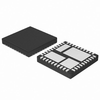
NCP3102MNTXG ON Semiconductor, NCP3102MNTXG Datasheet - Page 10

NCP3102MNTXG
Manufacturer Part Number
NCP3102MNTXG
Description
IC CONV SYNC BUCK 10A 40QFN
Manufacturer
ON Semiconductor
Type
Step-Down (Buck)r
Datasheet
1.NCP3102BMNTXG.pdf
(18 pages)
Specifications of NCP3102MNTXG
Internal Switch(s)
Yes
Synchronous Rectifier
Yes
Number Of Outputs
1
Voltage - Output
Adj to 0.8V
Current - Output
10A
Frequency - Switching
275kHz
Voltage - Input
4.5 ~ 13.2 V
Operating Temperature
0°C ~ 70°C
Mounting Type
Surface Mount
Package / Case
40-TQFN Exposed Pad
Power - Output
3W
Lead Free Status / RoHS Status
Lead free / RoHS Compliant
Other names
NCP3102MNTXGOSTR
Error(%) +
Error = R2 * 1.25 * 10
the desired output voltage as shown in the following
equation:
R3 +
voltages.
transconductance error amplifier (OTA). The compensation
network consists of the internal error amplifier and the
impedance networks ZIN (R3) and external ZFB (R
C
provide a closed loop transfer function with the highest 0 dB
crossing frequency to have fast response (but always lower
than f
minimize the load regulation. A stable control loop has a
gain crossing with -20 dB/decade slope and a phase margin
greater than 45°. Include worst-case component variations
when determining phase margin. Loop stability is defined by
C
SOFT-START
Table 2. OUTPUT VOLTAGES AND DIVIDER
RESISTORS
comp
V
Once R2 is calculated above R3 can be calculated to select
Table 2 shows R3 values for frequently used output
Figure 18 shows a typical Type II operational
OUT
0.8
1.0
1.2
1.5
1.8
2.5
3.3
5.0
V
SW
(V)
and C
OUT
/8) and the highest gain in DC conditions to
V
R2
R3
R2 * I
* V
REF
V
soft-start
R2 (kW
V
out
0.51
0.75
REF
C
1.8
1.3
1.6
1.6
1.6
2.7
COMP
R
REF
comp
comp
bias
DIS
Figure 18. FB circuit
FB
16
17
)
* R2
). The compensation network has to
* 100
-5
V
REF
R3 (kW) E24
(%)
None
0.75
0.51
0.51
2.0
1.5
1.5
1.3
0.8V
+
-
-
+
UVLO
VCC
POR
13
FAULT
R3 (kW) Calculated
2.040
1.500
1.486
1.280
0.753
0.512
0.514
None
(eq. 10)
(eq. 11)
http://onsemi.com
comp
NCP3102
,
10
the compensation network around the OTA, the output
capacitor, output inductor and the output divider. Figure 19
shows the open loop and closed loop gain plots. It is possible
to use Compensation Calculator Software Tool from
ON Semiconductor website. This tool can be downloaded
from http://www.onsemi.com.
Thermal Considerations
specifications section of this data sheet and a calculation can
be made to determine the NCP3102 junction temperature.
However, it should be noted that the physical layout of the
board, the proximity of other heat sources such as MOSFETs
and inductors, and the amount of metal connected to the
NCP3102, impact the temperature of the device. The PCB
is used also as the heatsink. Double or multi layer PCBs with
thermal vias between places with the same electrical
potential increase cooling area. A 70 mm thick copper
plating is a good solution to eliminate the need for an
external heatsink.
Layout Considerations
layout is very important. Using a good layout can solve
many problems associated with these types of power
supplies as transient occur.
for converter stability. They should be placed close to the
NCP3102. The feedback trace is recommended to be kept as
far from the inductor and noisy power traces as possible. The
resistor divider and feedback acceleration circuit (R2, R3,
R6, C13) is recommended to be placed near to input FB
(Pin 16, NCP3102).
generate voltage transients across the impedances of the
interconnecting bond wires and circuit traces. These
interconnecting impedances should be minimized by using
wide, short printed circuit traces. The critical components
should be located together as close as possible using ground
plane construction or single point grounding. The inductor
and output capacitors should be located together as close as
possible to the NCP3102.
The package thermal resistance can be obtained from the
When designing a high frequency switching converter,
External compensation components (R1, C9) are needed
Switching current from one power device to another can
100
A
Figure 19. Gain Plot for the Error Amplifier
F
Z
Unloaded Gain
1000
Closed Loop,
Gain = GMR
Compensation Network
FREQUENCY (Hz)
Open Loop, Unloaded Gain
10 k
1
F
P
100 k
B
Error Amplifier
1000 k


