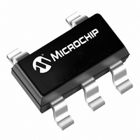
TCM828ECT713 Microchip Technology, TCM828ECT713 Datasheet - Page 14

TCM828ECT713
Manufacturer Part Number
TCM828ECT713
Description
IC CHARGE PUMP CONV SOT23A-5
Manufacturer
Microchip Technology
Type
Switched Capacitor (Charge Pump), Doubler, Invertingr
Specifications of TCM828ECT713
Package / Case
SOT-23-5, SC-74A, SOT-25
Internal Switch(s)
Yes
Synchronous Rectifier
No
Number Of Outputs
1
Voltage - Output
-1.5 ~ -5.5 V, ±3 ~ ±11 V
Current - Output
25mA
Frequency - Switching
12kHz
Voltage - Input
1.5 ~ 5.5 V
Operating Temperature
-40°C ~ 85°C
Mounting Type
Surface Mount
Power - Output
240mW
Minimum Operating Temperature
- 40 C
Mounting Style
SMD/SMT
Function
Inverting, Step Up
Output Voltage
- 1.5 V to - 5.5 V, 3 V to 11 V
Output Current
25 mA
Maximum Operating Temperature
85 C
Lead Free Status / RoHS Status
Lead free / RoHS Compliant
Lead Free Status / RoHS Status
Lead free / RoHS Compliant, Lead free / RoHS Compliant
Other names
158-2031-2
158-2031-2
TCM828ECT713TR
158-2031-2
TCM828ECT713TR
Available stocks
Company
Part Number
Manufacturer
Quantity
Price
Company:
Part Number:
TCM828ECT713
Manufacturer:
MICROCHIP
Quantity:
12 000
Part Number:
TCM828ECT713
Manufacturer:
MICROCHIP/微芯
Quantity:
20 000
TCM828/TCM829
5.0.3
In order to maintain the lowest output resistance and
output ripple voltage, it is recommended that low ESR
capacitors be used. Additionally, larger values of C1 will
lower the output resistance and larger values of C2 will
reduce output ripple. (See
Table 5-1
corresponding output resistance values @ +25°C. It
assumes a 0.1Ω ESR
the output voltage ripple for various values of C2. The
V
0.1Ω ESR
TABLE 5-1:
I
TABLE 5-2:
5.0.4
The V
reduce AC impedance and minimize noise effects due
to the switching internal to the device. The
recommended capacitor depends on the configuration
of the TCM828/TCM829 devices.
If the device is loaded from OUT to GND, it is
recommended that a large value capacitor (at least
equal to C1) be connected from the input to GND. If the
device is loaded from IN to OUT, a small (0.1 µF)
capacitor is sufficient.
DS21488B-page 14
C1 (µF)
C2 (µF)
RIPPLE
100
100
0.1
3.3
3.3
10
47
10
47
1
1
IN
values assume 10 mA output load current and
C2
input should be capacitively bypassed to
shows various values of C1 and the
CAPACITOR SELECTION
INPUT SUPPLY BYPASSING
TCM828 R
.
TCM828 V
OUTPUT RESISTANCE VS. C1
(ESR = 0.1Ω)
OUTPUT VOLTAGE RIPPLE
VS. C2 (ESR = 0.1Ω) IOUT
10MA
(mV)
850
100
835
254
42
25
18
17
85
20
10
C1
OUT
RIPPLE
and 2Ω R
Equation
(Ω)
SW
TCM829 R
TCM829 R
5-1).
.
Table 5-2
302
286
45
25
19
17
17
88
31
8
5
OUT
OUT
shows
(Ω)
(Ω)
5.0.5
The most common application for charge pump
devices is the inverter
uses two external capacitors – C1 and C2 (plus a
power supply bypass capacitor, if necessary). The
output is equal to V
loading. Refer to
selection.
FIGURE 5-3:
5.0.6
Two or more TCM828/829 devices can be cascaded to
increase output voltage
lightly loaded, it will be close to (– 2 x VIN) but will droop
at least by R
of the second. It can be seen that the output resistance
rises rapidly for multiple cascaded devices. For large
negative voltage requirements see the TC682 or
TCM680 data sheets.
FIGURE 5-4:
TCM829 Devices to Increase Output Voltage.
C1
*10 µF (TCM828)
3
1
2
IN
OUT
C1
3
4
5
-
VOLTAGE INVERTER
CASCADING DEVICES
OUT
TCM828/
TCM829
"1"
GND
of the first device multiplied by the IQ
Table 5-1
3.3 µF*
C1
Voltage Inverter
–
+
C3
IN
3.3 µF*
4
5
Test Circuit.
Cascading TCM828 or
2
1
C1
plus any voltage drops, due to
© 2010 Microchip Technology Inc.
C1
(Figure
V
(Table
+
and
IN
. . .
. . .
C2
3
4
5
Table 5-1
V
5-3). This application
5-4). If the output is
OUT
3.3 µF*
TCM828/
TCM829
C2
V
R
"n"
= -nV
OUT
L
for capacitor
IN
1
2
V
C2
V
OUT
OUT


