LM2585T-3.3/NOPB National Semiconductor, LM2585T-3.3/NOPB Datasheet
LM2585T-3.3/NOPB
Specifications of LM2585T-3.3/NOPB
*LM2585T-3.3/NOPB
LM2585T-3.3


Related parts for LM2585T-3.3/NOPB


LM2585T-3.3/NOPB Summary of contents
Page 1
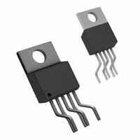
... Typical Applications ■ Flyback regulator ■ Multiple-output regulator ■ Simple boost regulator ■ Forward converter 1251514 Order Number LM2585T-3.3, LM2585T-5.0, LM2585T-12 or LM2585T-ADJ See NS Package Number T05D 1251516 12515 February 2, 2010 Bent, Staggered Leads 5-Lead TO-220 (T) Side View 1251515 5-Lead TO-263 (S) ...
Page 2
... Ordering Information Package Type 5-Lead TO-220 Bent, Staggered Leads 5-Lead TO-263 5-Lead TO-263 Tape and Reel www.national.com NSC Package Drawing T05D LM2585T-3.3, LM2585T-5.0, LM2585T-12, LM2585T-ADJ TS5B LM2585S-3.3, LM2585S-5.0, LM2585S-12, LM2585S-ADJ TS5B LM2585SX-3.3, LM2585SX-5.0, LM2585SX-12, LM2585SX-ADJ 2 Order Number ...
Page 3
... Absolute Maximum Ratings If Military/Aerospace specified devices are required, please contact the National Semiconductor Sales Office/ Distributors for availability and specifications. Input Voltage Switch Voltage Switch Current (Note 2) Compensation Pin Voltage Feedback Pin Voltage Storage Temperature Range Lead Temperature (Soldering, 10 sec.) Electrical Characteristics LM2585-3 ...
Page 4
LM2585-5.0 Symbol Parameters SYSTEM PARAMETERS Test Circuit of V Output Voltage OUT ΔV Line Regulation / OUT ΔV IN ΔV Load Regulation / OUT ΔI LOAD η Efficiency UNIQUE DEVICE PARAMETERS (Note V Output Reference REF Voltage ΔV Reference Voltage ...
Page 5
LM2585-ADJ Symbol Parameters SYSTEM PARAMETERS Test Circuit of V Output Voltage V OUT I LOAD ΔV Line Regulation V / OUT ΔV I LOAD IN ΔV Load Regulation V / OUT ΔI I LOAD LOAD η Efficiency V UNIQUE DEVICE ...
Page 6
Symbol Parameters I Switch Leakage L Current V Switch Sustaining SUS Voltage V Switch Saturation SAT Voltage I NPN Switch CL Current Limit θ Thermal Resistance JA θ JA θ JC θ JA θ JA θ JA θ JC Note ...
Page 7
Typical Performance Characteristics Supply Current vs Temperature ΔReference Voltage vs Supply Voltage Current Limit vs Temperature 1251502 1251504 Current vs Temperature 1251506 7 Reference Voltage vs Temperature 1251503 Supply Current vs Switch Current 1251505 Feedback Pin Bias 1251507 www.national.com ...
Page 8
Switch Saturation Voltage vs Temperature Oscillator Frequency vs Temperature Error Amp Voltage Gain vs Temperature www.national.com Switch Transconductance 1251508 Error Amp Transconductance 1251510 Short Circuit Frequency 1251512 8 vs Temperature 1251509 vs Temperature 1251511 vs Temperature 1251513 ...
Page 9
Flyback Regulator Block Diagram For Fixed Versions 3.3V 3.4k 5V 6.15k 12V 8.73k For Adj. Version R1 = Short (0Ω), R2 = Open FIGURE 1. ...
Page 10
Test Circuits —100 μF, 25V Aluminum Electrolytic C IN1 —0.1 μF Ceramic C IN2 T—22 μH, 1:1 Schott #67141450 D—1N5820 —680 μF, 16V Aluminum Electrolytic C OUT —0.47 μF Ceramic —2k C —100 μF, 25V Aluminum Electrolytic ...
Page 11
Flyback Regulator Operation The LM2585 is ideally suited for use in the flyback regulator topology. The flyback regulator can produce a single output voltage, such as the one shown in Figure voltages. In Figure 4, the flyback regulator generates an ...
Page 12
A: Switch Voltage, 20 V/div B: Switch Current, 2 A/div C: Output Rectifier Current, 2 A/div D: Output Ripple Voltage, 50 mV/div AC-Coupled Horizontal: 2 μs/div www.national.com FIGURE 5. Switching Waveforms FIGURE 6. V Load Current Step Response OUT 12 ...
Page 13
Typical Flyback Regulator Applications Figure 7 through Figure 12 show six typical flyback applica- tions, varying from single output to triple output. Each drawing contains the part number(s) and manufacturer(s) for every component except the transformer. For the transformer part ...
Page 14
FIGURE 9. Single-Output Flyback Regulator FIGURE 10. Dual-Output Flyback Regulator 14 1251526 1251527 ...
Page 15
FIGURE 11. Dual-Output Flyback Regulator FIGURE 12. Triple-Output Flyback Regulator 15 1251528 1251529 www.national.com ...
Page 16
TRANSFORMER SELECTION (T) Figure 13 lists the standard transformers available for flyback regulator applications. Included in the table are the turns ratio Applications Figure 7 Transformers T7 V 4V– 3.3V OUT1 I (Max) 1.4A OUT1 ...
Page 17
TRANSFORMER FOOTPRINTS Figure 15 through Figure 29 show the footprints of each trans- former, listed in Figure 14. T7 Top View FIGURE 15. Coilcraft S6000-A T6 Top View FIGURE 16. Coilcraft Q4339-B T5 Top View FIGURE 17. Coilcraft Q4437-B (Surface ...
Page 18
T5 Top View FIGURE 23. Pulse PE-68413 (Surface Mount) T7 Top View FIGURE 24. Renco RL-5751 T6 Top View FIGURE 25. Renco RL-5533 T5 Top View FIGURE 26. Renco RL-5532 www.national.com 1251539 FIGURE 28. Schott 67140900 1251540 1251542 FIGURE 29. ...
Page 19
By adding a small number of external components (as shown in the applied input voltage. The switching waveforms observed during the operation of this circuit are shown in shown in Figure 32. A: Switch Voltage, 10 V/div B: Switch Current, ...
Page 20
Typical Boost Regulator Applications Figure 33 and Figure 35 through Figure 37 boost applications)—one fixed and three using the adjustable version of the LM2585. Each drawing contains the part num- Figure 34 contains a table of standard inductors, by part ...
Page 21
LM2585 will require a heat sink in these applications. The size of the heat sink will depend on the maximum ambient temperature. To calculate the thermal resistance of the IC and the size of the heat sink needed, see ...
Page 22
Application Hints PROGRAMMING OUTPUT VOLTAGE (SELECTING R AND Referring to the adjustable regulator in voltage is programmed by the resistors R lowing formula OUT REF 1 2 Resistors ...
Page 23
FLYBACK REGULATOR INPUT CAPACITORS A flyback regulator draws discontinuous pulses of current from the input supply. Therefore, there are two input capaci- tors needed in a flyback regulator; one for energy storage and one for filtering (see Figure 39). Both ...
Page 24
... To further simplify the flyback regulator design procedure, National Semiconductor is making available computer design is the output voltage, OUT software to be used with the Simple Switcher line of switching regulators. Switchers Made Simple is available on a 3½ ...
Page 25
European Magnetic Vendor Contacts Please contact the following addresses for details of local distributors or representatives: Coilcraft 21 Napier Place Wardpark North Cumbernauld, Scotland G68 0LL Phone: +44 1236 730 595 Fax: +44 1236 730 627 Pulse Engineering Dunmore Road ...
Page 26
... Physical Dimensions www.national.com inches (millimeters) unless otherwise noted Order Number LM2585T-3.3, LM2585T-5.0, LM2585T-12 or LM2585T-ADJ NS Package Number T05D 26 ...
Page 27
Order Number LM2585S-3.3, LM2585S-5.0, LM2585S-12 or LM2585S-ADJ NS Package Number TS5B 27 www.national.com ...
Page 28
... For more National Semiconductor product information and proven design tools, visit the following Web sites at: www.national.com Products Amplifiers www.national.com/amplifiers Audio www.national.com/audio Clock and Timing www.national.com/timing Data Converters www.national.com/adc Interface www.national.com/interface LVDS www.national.com/lvds Power Management www.national.com/power Switching Regulators www.national.com/switchers LDOs www.national.com/ldo LED Lighting www ...