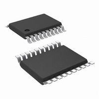
LM20343MH/NOPB National Semiconductor, LM20343MH/NOPB Datasheet - Page 13

LM20343MH/NOPB
Manufacturer Part Number
LM20343MH/NOPB
Description
IC REG SYNC BUCK 3A 20TSSOP
Manufacturer
National Semiconductor
Series
PowerWise®r
Type
Step-Down (Buck)r
Datasheet
1.LM20343MHNOPB.pdf
(20 pages)
Specifications of LM20343MH/NOPB
Internal Switch(s)
Yes
Synchronous Rectifier
Yes
Number Of Outputs
1
Voltage - Output
0.8 ~ 32 V
Current - Output
3A
Frequency - Switching
250kHz, 750kHz
Voltage - Input
4.5 ~ 36 V
Operating Temperature
-40°C ~ 125°C
Mounting Type
Surface Mount
Package / Case
20-TSSOP Exposed Pad, 20-eTSSOP, 20-HTSSOP
Primary Input Voltage
36V
No. Of Outputs
1
Output Voltage
32V
Output Current
3A
No. Of Pins
20
Operating Temperature Range
-40°C To +125°C
Msl
MSL 1 - Unlimited
Filter Terminals
SMD
Rohs Compliant
Yes
For Use With
LM20343EVAL - EVALUATION BOARD FOR THE LM20343
Lead Free Status / RoHS Status
Lead free / RoHS Compliant
Power - Output
-
Other names
*LM20343MH
*LM20343MH/NOPB
LM20343MH
*LM20343MH/NOPB
LM20343MH
The power stage transfer function is dictated by the modula-
tor, output LC filter, and load; while the feedback transfer
function is set by the feedback resistor ratio, error amp gain
and external compensation network.
To achieve a -20dB/decade slope, the error amplifier zero,
located at f
ter pole (f
Compensation of the LM20343 is achieved by adding an RC
network as shown in Figure 4 below.
A good starting value for C
Once the value of C
approximated using the equation below to cancel the output
filter pole (f
FIGURE 4. Compensation Network for LM20343
FIGURE 3. LM20343 Loop Compensation
P(FIL)
Z(EA)
P(FIL)
).
, should be positioned to cancel the output fil-
) as shown in Figure 3.
C1
is chosen the value of RC should be
C1
for most applications is 2.2 nF.
30051745
30051772
13
A higher crossover frequency can be obtained, usually at the
expense of phase margin, by lowering the value of C
recalculating the value of R
recalculating R
lower crossover frequency. As with any attempt to compen-
sate the LM20343 the stability of the system should be verified
for desired transient droop and settling time.
For low duty cycle operation, when the on time of the switch
node is less than 200ns, an additional capacitor (C
be added from the COMP pin to AGND. The recommended
value of this capacitor is 20pF. If low duty cycle jitter on the
switch node is observed, the value of this capacitor can be
increased to improve noise immunity; however, values much
larger than 100pF will cause the pole f
frequency degrading loop stability.
BOOT CAPACITOR (C
The LM20343 integrates an N-channel buck switch and as-
sociated floating high voltage level shift / gate driver. This gate
driver circuit works in conjunction with an internal diode and
an external bootstrap capacitor. A 0.1 µF ceramic capacitor,
connected with short traces between the BOOT pin and SW
pin, is recommended. During the off-time of the buck switch,
the SW pin voltage is approximately 0V and the bootstrap ca-
pacitor is charged from VCC through the internal bootstrap
diode.
SUB-REGULATOR BYPASS CAPACITOR (C
The capacitor at the VCC pin provides noise filtering for the
internal sub-regulator. The recommended value of C
should be no smaller than 0.1 µF and no greater than 1 µF.
The capacitor should be a good quality ceramic X5R or X7R
capacitor. In general, a 1 µF ceramic capacitor is recom-
mended for most applications. The VCC regulator should not
be used for other functions since it isn't protected against
short circuit.
SETTING THE START UP TIME (C
The addition of a capacitor connected from the SS pin to
ground sets the time at which the output voltage will reach the
final regulated value. Larger values for C
start up times. Table 3, shown below provides a list of soft
start capacitors and the corresponding typical start up times.
If different start up times are needed the equation shown be-
low can be used to calculate the start up time.
As shown above, the start up time is influenced by the value
of the soft-start capacitor C
current I
While the soft-start capacitor can be sized to meet many start
up requirements, there are limitations to its size. The soft-start
TABLE 3. Start Up Times for Different Soft-Start
Start Up Time (ms)
SS
.
10
15
20
1
5
C1
will provide additional phase margin at a
BOOT
Capacitors
C1
SS
)
. Likewise, increasing C
and the 4.5 µA soft-start pin
SS
P2(EA)
)
SS
C
will result in longer
to move to a lower
SS
none
100
120
33
68
(nF)
VCC
www.national.com
C2
)
) should
C1
C1
and
and
VCC


