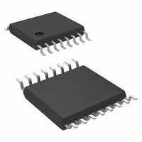
LM20143MH/NOPB National Semiconductor, LM20143MH/NOPB Datasheet - Page 14

LM20143MH/NOPB
Manufacturer Part Number
LM20143MH/NOPB
Description
IC REG SYNC BUCK 3A ADJ 16TSSOP
Manufacturer
National Semiconductor
Series
PowerWise®r
Type
Step-Down (Buck)r
Datasheet
1.LM20143MHNOPB.pdf
(20 pages)
Specifications of LM20143MH/NOPB
Internal Switch(s)
Yes
Synchronous Rectifier
Yes
Number Of Outputs
1
Voltage - Output
0.8 ~ 5 V
Current - Output
3A
Frequency - Switching
500kHz ~ 1.5MHz
Voltage - Input
2.95 ~ 5.5 V
Operating Temperature
-40°C ~ 125°C
Mounting Type
Surface Mount
Package / Case
16-TSSOP Exposed Pad, 16-eTSSOP, 16-HTSSOP
Power - Output
2.6W
For Use With
LM20143EVAL - BOARD EVAL 3A POWERWISE LM20143
Lead Free Status / RoHS Status
Lead free / RoHS Compliant
Other names
*LM20143MH/NOPB
LM20143MH
LM20143MH
www.national.com
The power stage transfer function is dictated by the modula-
tor, output LC filter, and load; while the feedback transfer
function is set by the feedback resistor ratio, error amp gain,
and external compensation network.
To achieve a -20dB/decade slope, the error amplifier zero,
located at f
pole (f
can be added to cancel the output filter zero at f
cellation of the output filter zero is recommended if larger
value, non-ceramic output capacitors are used.
Compensation of the LM20143 is achieved by adding an RC
network as shown in Figure 5 below.
A good starting value for C
Once the value of C
calculated using the equation below to cancel the output filter
pole (f
FIGURE 5. Compensation Network for LM20143
P(FIL)
P(FIL)
FIGURE 4. LM20143 Loop Compensation
) as shown in Figure 4.
). An additional error amp pole, located at f
Z(EA)
, should positioned to cancel the output filter
C1
is chosen the value of RC should be
C1
for most applications is 4.7 nF.
30030514
Z(FIL)
30030513
. Can-
P2(EA)
,
14
A higher crossover frequency can be obtained, usually at the
expense of phase margin, by lowering the value of C
recalculating the value of R
recalculating R
lower crossover frequency. As with any attempt to compen-
sate the LM20143 the stability of the system should be verified
for desired transient droop and settling time.
If the output filter zero, f
quency (F
at the COMP pin to ground. This capacitor adds a pole to
cancel the output filter zero assuring the crossover frequency
will occur before the double pole at f
margin. The output filter zero is set by the output capacitor
value and ESR as shown in the equation below.
If needed, the value for C
equation shown below.
Where R
R
AVIN FILTERING COMPONENTS (C
To prevent high frequency noise spikes from disturbing the
sensitive analog circuitry connected to the AVIN and AGND
pins, a high frequency RC filter is required between PVIN and
AVIN. These components are shown in Figure 2. as C
R
ommended value of C
should be placed as close to the IC as possible with a direct
connection from AVIN to AGND. A good quality X5R or X7R
ceramic capacitor should be used for C
SUB-REGULATOR BYPASS CAPACITOR (C
The capacitor at the VCC pin provides noise filtering and sta-
bility for the internal sub-regulator. The recommended value
of C
10 µF. The capacitor should be a good quality ceramic X5R
or X7R capacitor. In general, a 1 µF ceramic capacitor is rec-
ommended for most applications.
SETTING THE START UP TIME (C
The addition of a capacitor connected from the SS pin to
ground sets the time at which the output voltage will reach the
final regulated value. Larger values for C
start up times. Table 3, shown below provides a list of soft
start capacitors and the corresponding typical start up times.
C1
F
. The required value for R
VCC
is the calculated compensation resistance.
TABLE 3. Start Up Times for Different Soft-Start
Start Up Time (ms)
should be no smaller than 1 µF and no greater than
ESR
C
), an additional capacitor (C
is the output capacitor series resistance and
10
15
20
1
5
C1
will provide additional phase margin at a
F
Capacitors
Z(FIL)
is 1.0 µF. The filter capacitor, C
C2
C1
F
should be calculated using the
. Likewise, increasing C
approaches the crossover fre-
is 1Ω. C
SW
SS
F
/2 degrades the phase
)
F
F
C2
and R
SS
.
must be used. Rec-
C
) should be placed
will result in longer
SS
none
100
120
33
68
(nF)
F
)
VCC
)
C1
C1
F
and
and
and
F


