ISL8510IRZ Intersil, ISL8510IRZ Datasheet
ISL8510IRZ
Specifications of ISL8510IRZ
Available stocks


Related parts for ISL8510IRZ

ISL8510IRZ Summary of contents
Page 1
... CAUTION: These devices are sensitive to electrostatic discharge; follow proper IC Handling Procedures. | 1-888-INTERSIL or 1-888-468-3774 Intersil (and design registered trademark of Intersil Americas Inc. Copyright © Intersil Americas Inc. 2007, 2008. All Rights Reserved All other trademarks mentioned are the property of their respective owners. ...
Page 2
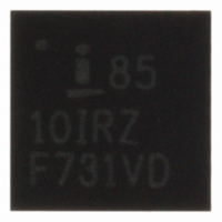
... ISL8510 Ordering Information PART NUMBER (Note) ISL8510IRZ* 85 10IRZ *Add “-T” suffix for tape and reel. Please refer to TB347 for details reel specifications. 18 VIN NOTE: These Intersil Pb-free plastic packaged products employ special Pb-free material sets, molding compounds/die attach 17 VIN materials, and 100% matte tin plate plus anneal (e3 termination ...
Page 3
Typical Application Schematics R5 5.11k FB_LDO R6 5.11k LDO 1.2V VOUT C6 22µF VIN_LDO VOUT1 C7 10µF 3 ISL8510 R2 2.21k C4 C5 0.1µF 0.033µF ISL8510 C14 1µF FIGURE 1. V RANGE FROM 4. 301 ...
Page 4
Typical Application Schematics 0.1 µ 5.11k FB_LDO LDO R6 5.11k VOUT 1. µ F VIN_LDO VOUT C7 10 µ ISL8510 (Continued) R2 2.21k C4 C5 0.033 µ F ISL8510 C14 1 µ F FIGURE ...
Page 5
Functional Block Diagram VCC SOFT-START CONTROL 30µA SS EN_PWM EN_LDO VIN LDO VCC PG_PWM PG_LDO GND 5 ISL8510 VOLTAGE - + MONITOR EA 0.6V RAMP REFERENCE GENERATOR FAULT THERMAL MONITOR MONITOR OSCILLATOR +150°C OC MONITOR PVCC POWER-ON RESET VIN_LDO MONITOR ...
Page 6
... Maximum Junction Temperature (Plastic Package +150°C Maximum Storage Temperature Range . . . . . . . . . .-65°C to +150°C Ambient Temperature Range .-40°C to +85°C Junction Temperature Range .-40°C to +125°C Pb-free Reflow Profile . . . . . . . . . . . . . . . . . . . . . . . See Link Below http://www.intersil.com/pbfree/Pb-FreeReflow.asp SYMBOL TEST CONDITIONS VIN VIN connected to VCC ...
Page 7
Electrical Specifications Unless Otherwise Noted, Typical Specifications are Measured at the Following Conditions 25V. Parameters with MIN and/or MAX limits are 100% tested at +25°C, unless otherwise specified. IN Temperature limits established by characterization and ...
Page 8
Pin Descriptions FB_LDO 1 VOUT 2 VIN_LDO 3 25 GND GND 4 GND VIN The input supply for the PWM regulator power stage and the source for ...
Page 9
Typical Performance Curves 100 1.8V 60 OUT 2.5V OUT 50 1.5V OUT 40 1.2V OUT 0.00 0.25 0.50 0.75 OUTPUT LOAD (A) FIGURE 3. EFFICIENCY vs LOAD 3.3V ...
Page 10
Typical Performance Curves 2.503 2.502 2.501 12V IN 2.500 0.00 0.25 0.50 0.75 OUTPUT LOAD (A) FIGURE 9. V REGULATION vs LOAD, 500kHz 2.5V OUT 5.015 5.014 5.013 7V IN 5.012 5.011 5.010 5.009 5.008 12V IN 5.007 25V 5.006 ...
Page 11
Typical Performance Curves 5.1 5.0 4.9 4.8 4.7 4.6 4.5 4 100 I V (mA) CC FIGURE 15. V LOAD REGULATION CC LX 5V/DIV V RIPPLE OUT 20mV/DIV IL 0.2A/DIV LDO RIPPLE 20mV/DIV FIGURE 18. STEADY STATE OPERATION ...
Page 12
Typical Performance Curves LX 5V/DIV V RIPPLE OUT 100mV/DIV IL 1A/DIV LDO RIPPLE 20mV/DIV FIGURE 20. LOAD TRANSIENT, 200µs/DIV EN 5V/DIV IL 1A/DIV PG_PWM 2V/DIV SS 2V/DIV FIGURE 22. SOFT-START AT FULL LOAD, 500µs/DIV EN 5V/DIV IL 1A/DIV PG_PWM 5V/DIV ...
Page 13
Typical Performance Curves IL 1A/DIV FIGURE 26. OUTPUT SHORT CIRCUIT, 5µs/DIV FIGURE 28. LDO SHORT CIRCUIT AND RECOVERY, 200µs/DIV 13 ISL8510 Circuit of Figure 12V, VIN_LDO = -40°C to +85°C, unless otherwise noted. ...
Page 14
Detailed Description The ISL8510 combines a standard buck PWM controller with an integrated switching MOSFET and one low dropout (LDO) linear regulators with internal pass devices. The buck controller drives an internal N-Channel MOSFET and requires an external diode to ...
Page 15
This linear ramp is applied to the non-inverting input of the internal error amplifier and overrides the nominal 0.6V reference. The output voltage reaches its regulation ...
Page 16
LDO Current Limit The ISL8510 monitors and controls the pass transistor’s gate voltage to limit output current. The current limit for LDO is 700mA typical. The output can be shorted to ground without damaging the part due to the current ...
Page 17
ESR of 50mΩ or less to insure stability and optimum transient response. For stable operation, a ceramic capacitor, with a minimum value of 10µF, is recommended for LDO output. There is no upper limit to the output capacitor ...
Page 18
MOSFET turns on. Place the small ceramic capacitors physically close to the MOSFET VIN pins (switching MOSFET drain) and the Schottky diode anode. The important parameters for the bulk input capacitance ...
Page 19
... A more detailed explanation of voltage mode control of a buck regulator can be found in Tech Brief TB417, entitled “Designing Stable Compensation Networks for Single Phase Voltage Mode Buck Regulators.” http://www.intersil.com/data/tb/tb417.pdf Layout Considerations Layout is very important in high frequency switching converter design. With power devices switching efficiently at ...
Page 20
... Accordingly, the reader is cautioned to verify that data sheets are current before placing orders. Information furnished by Intersil is believed to be accurate and reliable. However, no responsibility is assumed by Intersil or its subsidiaries for its use; nor for any infringements of patents or other rights of third parties which may result from its use ...
Page 21
Package Outline Drawing L24.4x4D 24 LEAD QUAD FLAT NO-LEAD PLASTIC PACKAGE Rev 2, 10/06 4.00 PIN 1 INDEX AREA (4X) 0.15 TOP VIEW ( TYP ) ( TYPICAL RECOMMENDED LAND PATTERN 21 ISL8510 ...