LM2596S-ADJ/NOPB National Semiconductor, LM2596S-ADJ/NOPB Datasheet - Page 4
LM2596S-ADJ/NOPB
Manufacturer Part Number
LM2596S-ADJ/NOPB
Description
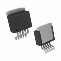
IC REG SIMPLE SWITCHER TO-263-5
Manufacturer
National Semiconductor
Series
SIMPLE SWITCHER®r
Type
Step-Down (Buck)r
Datasheets
1.LM2596S-ADJNOPB.pdf
(31 pages)
2.LM2587S-ADJNOPB.pdf
(28 pages)
3.LM2596S-ADJNOPB.pdf
(6 pages)
Specifications of LM2596S-ADJ/NOPB
Internal Switch(s)
Yes
Synchronous Rectifier
No
Number Of Outputs
1
Voltage - Output
1.2 ~ 37 V
Current - Output
3A
Frequency - Switching
150kHz
Voltage - Input
4.5 ~ 40 V
Operating Temperature
-40°C ~ 125°C
Mounting Type
Surface Mount
Package / Case
D²Pak, TO-263 (5 leads + tab)
Current, Input Bias
10 nA
Current, Output
3 A
Current, Supply
5 mA
Frequency, Oscillator
150 kHz
Package Type
TO-263
Regulator Type
Buck, Switching
Resistance, Thermal, Junction To Case
2 °C/W
Temperature, Operating, Range
-40 to +125 °C
Voltage, Input
4.5 to 40 V
Voltage, Output
1.2 to 37 V
Primary Input Voltage
40V
No. Of Outputs
1
Output Voltage
37V
Output Current
3A
No. Of Pins
5
Operating Temperature Range
-40°C To +125°C
Msl
MSL 3 - 168 Hours
Filter Terminals
SMD
Rohs Compliant
Yes
For Use With
551011367-041 - BOARD WEBENCH BUILD IT
Lead Free Status / RoHS Status
Lead free / RoHS Compliant
Power - Output
-
Lead Free Status / Rohs Status
RoHS Compliant part
Other names
*LM2596S-ADJ
*LM2596S-ADJ/NOPB
LM2596S-ADJ
*LM2596S-ADJ/NOPB
LM2596S-ADJ
Available stocks
Company
Part Number
Manufacturer
Quantity
Price
Company:

Part Number:
LM2596S-ADJ/NOPB
Manufacturer:
TI
Quantity:
25


www.national.com
SYSTEM PARAMETERS Test Circuit of
V
ΔV
ΔV
ΔV
ΔI
η
UNIQUE DEVICE PARAMETERS
V
ΔV
G
A
I
I
V
f
f
V
B
S
O
SC
Symbol
OUT
REF
VOL
UV
EAO
M
Symbol
LOAD
LM2587-ADJ
Electrical Characteristics
Specifications with standard type face are for T
Range. Unless otherwise specified, V
All Output Voltage Versions
Electrical Characteristics
Specifications with standard type face are for T
Range. Unless otherwise specified, V
OUT
IN
OUT
REF
/
/
Input Supply Current
Input Supply
Undervoltage Lockout
Oscillator Frequency
Short-Circuit
Frequency
Error Amplifier
Output Swing
Output Voltage
Line Regulation
Load Regulation
Efficiency
Output Reference
Voltage
Reference Voltage
Line Regulation
Error Amp
Transconductance
Error Amp
Voltage Gain
Error Amp
Input Bias Current
Parameters
Parameters
(Note
V
I
V
I
V
I
V
Measured at Feedback Pin
V
V
I
V
V
R
V
LOAD
LOAD
LOAD
COMP
(Switch Off)
(Note
I
R
Measured at Switch Pin
R
V
Measured at Switch Pin
R
V
Upper Limit
(Note
Lower Limit
(Note
IN
IN
IN
IN
COMP
IN
COMP
COMP
COMP
COMP
SWITCH
COMP
FEEDBACK
LOAD
LOAD
LOAD
IN
IN
Figure 3 (Note
= 4V to 10V
= 4V to 10V
= 10V
= 10V, I
5)
= 4V to 40V
= 5V.
= 5V.
= 300 mA to 1.2A
= 300 mA
= 300 mA to 1.2A
= −30 μA to +30 μA
= 1.0V
= 1.0V
= 0.5V to 1.6V
= 1.0 MΩ
= 1.0V
8)
7)
8)
= 100Ω
= 100Ω
= 100Ω
= 1.0V
= 3.0A
(Note
Conditions
LOAD
= 1.15V
J
J
= 25°C, and those in bold type face apply over full Operating Temperature
= 25°C, and those in bold type face apply over full Operating Temperature
5)
= 1A
(Note
Conditions
4)
6)
4
Typical
1.230
3.200
12.0
670
125
1.5
20
20
90
11.52/11.40
1.208/1.205
Typical
400/200
1.800
3.30
0.25
100
2.8
Min
11
85
25
2.6/2.4
85/75
3.05
Min
12.48/12.60
1.252/1.255
100/200
100/200
425/600
6.000
Max
15.5/16.5
0.40/0.55
140/165
115/125
Max
3.75
mmho
Units
Units
mV
mV
mV
V/V
nA
%
kHz
kHz
V
V
mA
mA
V
V
V
Related parts for LM2596S-ADJ/NOPB
Image
Part Number
Description
Manufacturer
Datasheet
Request
R

Part Number:
Description:
IC REG SIMPLE SWITCHER TO-263-5
Manufacturer:
National Semiconductor
Datasheet:
Part Number:
Description:
IC REG SIMPLE SWITCHER TO-263-5
Manufacturer:
National Semiconductor
Datasheet:
Part Number:
Description:
IC REG SIMPLE SWITCHER TO-263-5
Manufacturer:
National Semiconductor
Datasheet:

Part Number:
Description:
SWITCHING REG, 3A 3.3V, SMD, 2596
Manufacturer:
National Semiconductor
Datasheet:

Part Number:
Description:
DC/DC Converter IC
Manufacturer:
National Semiconductor
Datasheet:
Part Number:
Description:
DC/DC Converter IC
Manufacturer:
National Semiconductor
Datasheet:
Part Number:
Description:
DC/DC Converter IC
Manufacturer:
National Semiconductor
Datasheet:

Part Number:
Description:
National Semiconductor [8-Bit D/A Converter]
Manufacturer:
National Semiconductor
Datasheet:
Part Number:
Description:
National Semiconductor [Media Coprocessor]
Manufacturer:
National Semiconductor
Datasheet:
Part Number:
Description:
Digitally Controlled Tone and Volume Circuit with Stereo Audio Power Amplifier, Microphone Preamp Stage and National 3D Sound
Manufacturer:
National Semiconductor
Datasheet:
Part Number:
Description:
Digitally Controlled Tone and Volume Circuit with Stereo Audio Power Amplifier, Microphone Preamp Stage and National 3D Sound
Manufacturer:
National Semiconductor
Datasheet:
Part Number:
Description:
AC97 Rev 2 Codec with Sample Rate Conversion and National 3D Sound
Manufacturer:
National Semiconductor
Part Number:
Description:
Manufacturer:
National Semiconductor
Datasheet: