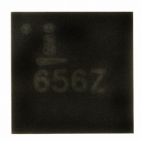
ISL97656IRTZ-TK Intersil, ISL97656IRTZ-TK Datasheet - Page 7

ISL97656IRTZ-TK
Manufacturer Part Number
ISL97656IRTZ-TK
Description
IC VREG STEP-UP HF/HE 10-TDFN
Manufacturer
Intersil
Type
Step-Up (Boost)r
Datasheet
1.ISL97656IRTZ-TK.pdf
(8 pages)
Specifications of ISL97656IRTZ-TK
Internal Switch(s)
Yes
Synchronous Rectifier
No
Number Of Outputs
1
Voltage - Output
5 ~ 25 V
Current - Output
1A
Frequency - Switching
640kHz, 1.2MHz
Voltage - Input
2.3 ~ 6 V
Operating Temperature
-40°C ~ 85°C
Mounting Type
Surface Mount
Package / Case
10-TDFN Exposed Pad
Rohs Compliant
YES
Lead Free Status / RoHS Status
Lead free / RoHS Compliant
Power - Output
-
Other names
ISL97656IRTZ-TK
Available stocks
Company
Part Number
Manufacturer
Quantity
Price
Part Number:
ISL97656IRTZ-TK
Manufacturer:
INTERSIL
Quantity:
20 000
I
Maximum Output Current
The MOSFET current limit is nominally 4.0A and guaranteed
3.8A. This restricts the maximum output current, I
based on Equation 7:
where:
ΔI
V
f
I
D = MOSFET turn-on ratio:
Table 1 gives typical maximum I
switching frequency and 10µH inductor.
Intersil products are sold by description only. Intersil Corporation reserves the right to make changes in circuit design, software and/or specifications at any time without
notice. Accordingly, the reader is cautioned to verify that data sheets are current before placing orders. Information furnished by Intersil is believed to be accurate and
reliable. However, no responsibility is assumed by Intersil or its subsidiaries for its use; nor for any infringements of patents or other rights of third parties which may result
from its use. No license is granted by implication or otherwise under any patent or patent rights of Intersil or its subsidiaries.
L
D
S
L-AVG
DIODE
L
=
I
I
ΔI
= switching frequency, 600kHz or 1.2MHz
=
L
L(AVG)
=
L
I
= MOSFET current limit
1
L AVG
= inductor ripple current
(
V
------------------------------------------------------------------------------
–
V
=
IN
--------------------------------------------
V
IN
L
= Schottky diode forward voltage, typically, 0.6V
2.5
2.5
2.5
3.3
3.3
3.3
TABLE 1. TYPICAL MAXIMUM I
OUT
5
5
I
-------------
1 D
×
= average inductor current
×
OUT
(V)
)
–
[
(
+
(
V
V
(
V
+
O
1 2 ⁄
O
All Intersil U.S. products are manufactured, assembled and tested utilizing ISO9000 quality systems.
IN
V
+
+
DIODE
V
V
×
DIODE
DIODE
Intersil Corporation’s quality certifications can be viewed at www.intersil.com/design/quality
ΔI
L
For information regarding Intersil Corporation and its products, see www.intersil.com
)
)
) V
V
×
–
OUT
f
S
12
12
12
5
9
5
9
9
IN
7
(V)
]
OUT
values for 1.2MHz
OUT
VALUES
I
OMAX
1790
2370
1300
1970
1470
990
750
970
OMAX
(mA)
(EQ. 10)
(EQ. 7)
(EQ. 8)
(EQ. 9)
,
ISL97656
Cascaded MOSFET Application
A 24V N-Channel MOSFET is integrated in the boost
regulator. For the applications where the output voltage is
greater than 24V, an external cascaded MOSFET is needed
as shown in Figure 11. The voltage rating of the external
MOSFET should be greater than A
DC PATH BLOCK APPLICATION
Note that there is a DC path in the boost converter from the
input to the output through the inductor and diode, hence the
input voltage will be seen at output with a forward voltage
drop of diode before the part is enabled. If this voltage is not
desired, the following circuit (see Figure 12) can be inserted
between input and inductor to disconnect the DC path when
the part is disabled.
FIGURE 12. CIRCUIT TO DISCONNECT THE DC PATH OF
TO INDUCTOR
FIGURE 11. CASCADED MOSFET TOPOLOGY FOR HIGH
V
IN
EN
BOOST CONVERTER
OUTPUT VOLTAGE APPLICATIONS
INTERSIL
ISL97656
LX
IN
FB
.
April 2, 2010
INPUT
FN6439.4
A
IN


