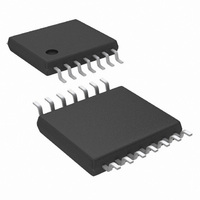
LM3150MHE/NOPB National Semiconductor, LM3150MHE/NOPB Datasheet - Page 10

LM3150MHE/NOPB
Manufacturer Part Number
LM3150MHE/NOPB
Description
IC REG SWITCH CTRL 6-42V 14TSSOP
Manufacturer
National Semiconductor
Series
PowerWise®, SIMPLE SWITCHER®r
Type
Step-Down (Buck)r
Datasheet
1.LM3150MHENOPB.pdf
(20 pages)
Specifications of LM3150MHE/NOPB
Internal Switch(s)
No
Synchronous Rectifier
Yes
Number Of Outputs
1
Voltage - Output
Adj to 0.6V
Current - Output
12A
Frequency - Switching
1MHz
Voltage - Input
6 ~ 42 V
Operating Temperature
-40°C ~ 125°C
Mounting Type
Surface Mount
Package / Case
14-TSSOP Exposed Pad, 14-eTSSOP 14-HTSSOP
Package
14TSSOP EP
Output Voltage
0.6(Min) V
Output Current
12(Max) A
For Use With
551600142-002 - WEBENCH BUILD IT BOARD LM3150
Lead Free Status / RoHS Status
Lead free / RoHS Compliant
Power - Output
-
Other names
LM3150MHETR
Available stocks
Company
Part Number
Manufacturer
Quantity
Price
Company:
Part Number:
LM3150MHE/NOPB
Manufacturer:
TI
Quantity:
17 600
Company:
Part Number:
LM3150MHE/NOPB
Manufacturer:
TI
Quantity:
11 235
Company:
Part Number:
LM3150MHE/NOPB
Manufacturer:
National Semiconductor
Quantity:
1 807
www.national.com
The soft-start time should be greater than the input voltage
rise time and also satisfy the following equality to maintain a
smooth transition of the output voltage to the programmed
regulation voltage during startup.
Enable/Shutdown
The EN pin can be activated by either leaving the pin floating
due to an internal pull up resistor to VIN or by applying a logic
high signal to the EN pin of 1.26V or greater. The LM3150 can
be remotely shut down by taking the EN pin below 1.02V. Low
quiescent shutdown is achieved when V
During low quiescent shutdown the internal bias circuitry is
turned off.
The LM3150 has certain fault conditions that can trigger shut-
down, such as over-voltage protection, current limit, under-
voltage lockout, or thermal shutdown. During shutdown, the
soft-start capacitor is discharged. Once the fault condition is
removed, the soft-start capacitor begins charging, allowing
the part to start-up in a controlled fashion. In conditions where
there may be an open drain connection to the EN pin, it may
be necessary to add a 1 nF bypass capacitor to this pin. This
will help decouple noise from the EN pin and prevent false
disabling.
Thermal Protection
The LM3150 should be operated such that the junction tem-
perature does not exceed the maximum operating junction
temperature. An internal thermal shutdown circuit, which ac-
tivates at 165°C (typical), takes the controller to a low-power
reset state by disabling the buck switch and the on-timer, and
grounding the SS pin. This feature helps prevent catastrophic
failures from accidental device overheating. When the junc-
tion temperature falls back below 150°C the SS pin is re-
leased and device operation resumes.
t
SS
≥
(V
OUT
x C
OUT
) / (I
OCL
- I
OUT
EN
)
is less than 0.4V.
(12)
10
Design Guide
The design guide provides the equations required to design
with
WEBENCH
section for a more complete and simplified design process.
1. Define Power Supply Operating Conditions
a. Required Output Voltage
b. Maximum and Minimum DC Input Voltage
c. Maximum Expected Load Current during Normal Operation
d. Soft-Start Time
2. Set Output Voltage With Feedback Resistors
where R
3. Determine R
The available frequency range for a given input voltage range,
is determined by the duty-cycle, D = V
mum t
teristics table. The maximum frequency is thus, f
t
The off-time will need to be less than the minimum off-time
t
turn off and turn on delays of the MOSFETs which can easily
add another 200 ns. The minimum off-time will occur at max-
imum duty cycle D
chosen will allow for the minimum desired input voltage. The
requirement for minimum off-time is t
MIN
necessary to choose a smaller switching frequency f
Choose R
input voltage matches your f
ing formula:
Use
the minimum desired input voltage. If the minimum desired
input voltage is not met, recalculate R
frequency.
ON-MIN
OFF
R
+ 200 ns). If t
ON
R
as specified in the electrical characteristics table plus any
Figure 2
OND
ON
the
. Where D
= [(V
FB1
and t
ON
= - [(V
®
is the bottom resistor and R
OUT
LM3150
FIGURE 2. Minimum V
design tool can be used with or in place of this
so that the switching frequency at your typical
to determine if the calculated R
OFF
ON
x V
min
IN
OFF
times as specified in the electrical charac-
- 1) x (V
and f
=V
IN
max
does not meet this requirement it will be
) - V
OUT
SIMPLE
and will determine if the frequency
s
I
OUT
/V
OUT
IN
IN-MAX
S
] / (V
x 16.5 + 100)] - 1000
= 10 A
chosen above using the follow-
, is the minimum duty-cycle.
IN
SWITCHER
x K x f
OFF
IN
ON
OUT
vs. V
FB2
= (1–D
for a lower switching
/V
S
is the top resistor.
) + R
OUT
IN
ON
, and the mini-
®
max
30053183
will allow for
OND
smax
)/f
Controller.
s
S
≥
= D
.
(t
(13)
(14)
(15)
OFF-
min
/


