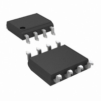
LM2594M-ADJ/NOPB National Semiconductor, LM2594M-ADJ/NOPB Datasheet - Page 3

LM2594M-ADJ/NOPB
Manufacturer Part Number
LM2594M-ADJ/NOPB
Description
IC REG SIMPLE SWITCHER 8-SOIC
Manufacturer
National Semiconductor
Series
SIMPLE SWITCHER®r
Type
Step-Down (Buck)r
Specifications of LM2594M-ADJ/NOPB
Internal Switch(s)
Yes
Synchronous Rectifier
No
Number Of Outputs
1
Voltage - Output
1.2 ~ 37 V
Current - Output
500mA
Frequency - Switching
150kHz
Voltage - Input
4.5 ~ 40 V
Operating Temperature
-40°C ~ 125°C
Mounting Type
Surface Mount
Package / Case
8-SOIC (3.9mm Width)
Primary Input Voltage
60V
No. Of Outputs
1
Output Voltage
37V
Output Current
500mA
No. Of Pins
8
Operating Temperature Range
-40°C To +125°C
Msl
MSL 1 - Unlimited
Rohs Compliant
Yes
Current, Input Bias
10 nA
Current, Output
0.5 A
Current, Supply
5 mA
Frequency, Oscillator
150 kHz
Package Type
SOIC
Regulator Type
Buck (Step-Down)
Temperature, Operating, Range
-40 to +125 °C
Voltage, Input
4.5 to 40 V
Voltage, Output
1.2 to 37 V
Peak Reflow Compatible (260 C)
Yes
Termination Type
SMD
Filter Terminals
SMD
Input Voltage
40V
Lead Free Status / RoHS Status
Lead free / RoHS Compliant
Power - Output
-
Lead Free Status / Rohs Status
RoHS Compliant part
Electrostatic Device
Other names
*LM2594M-ADJ
LM2594M-ADJ
LM2594M-ADJ
Available stocks
Company
Part Number
Manufacturer
Quantity
Price
Company:
Part Number:
LM2594M-ADJ/NOPB
Manufacturer:
National Semiconductor
Quantity:
1 940
Company:
Part Number:
LM2594M-ADJ/NOPB
Manufacturer:
NS/TI
Quantity:
70
Symbol
Symbol
SYSTEM PARAMETERS (Note 5) Test Circuit Figure 1
V
DEVICE PARAMETERS
I
f
V
DC
I
I
I
I
ON/OFF CONTROL Test Circuit Figure 1
V
V
I
I
b
O
CL
L
Q
STBY
H
L
LM2594/LM2594HV-ADJ
Electrical Characteristics
Specifications with standard type face are for T
ture Range
All Output Voltage Versions
Electrical Characteristics
JA
Note 1: Absolute Maximum Ratings indicate limits beyond which damage to the device may occur. Operating Ratings indicate conditions for which the device is in-
tended to be functional, but do not guarantee specific performance limits. For guaranteed specifications and test conditions, see the Electrical Characteristics.
FB
Specifications with standard type face are for T
ture Range . Unless otherwise specified, V
sion. I
SAT
IH
IL
LOAD
Feedback Bias Current
Oscillator Frequency
Saturation Voltage
Max Duty Cycle (ON)
Min Duty Cycle (OFF)
Current Limit
Output Leakage Current
Quiescent Current
Standby Quiescent
Current
Thermal Resistance
ON /OFF Pin Logic Input
Threshold Voltage
ON /OFF Pin
Input Current
Feedback Voltage
Efficiency
= 100 mA
Parameter
Parameter
4.5V
V
V
OUT
IN
= 12V, I
Adjustable Version Only, VFB = 1.3V
(Note 6)
I
(Note 8)
(Note 9)
Peak Current, (Note 7) (Note 8)
(Note 7) (Note 9) (Note 10)
(Note 9)
ON/OFF pin = 5V (OFF)
LM2594
LM2594HV
N Package, Junction to Ambient (Note 11)
M Package, Junction to Ambient (Note 11)
Low (Regulator ON)
High (Regulator OFF)
V
V
programmed for 3V. Circuit of Figure 1
OUT
V
LOGIC
LOGIC
IN
IN
= 0.5A (Note 7) (Note 8)
LOAD
= 12V for the 3.3V, 5V, and Adjustable version and V
V
= 2.5V (Regulator OFF)
= 0.5V (Regulator ON)
J
J
INmax
= 25˚C, and those with boldface type apply over full Operating Tempera-
= 25˚C, and those with boldface type apply over full Operating Tempera-
= 0.5A
Conditions
, 0.1A
Conditions
Output = −1V
I
LOAD
4
(Note 10)
0.5A
Output = 0V
(Note 3)
LM2594/LM2594HV-ADJ
1.230
LM2594/LM2594HV-XX
(Note 3)
Typ
80
0.02
Typ
150
100
140
150
0.9
0.8
1.3
10
85
95
0
2
5
5
IN
= 24V for the 12V ver-
1.193/1.180
1.267/1.280
0.65/0.58
(Note 4)
127/110
173/173
200/250
250/300
(Note 4)
1.1/1.2
1.3/1.4
50/100
Limit
Limit
0.6
2.0
50
15
10
15
5
kHz(max)
kHz(min)
mA(max)
mA(max)
µA(max)
µA(max)
µA(max)
µA(max)
µA(max)
(Limits)
V(max)
A(max)
V(max)
(Limits)
A(min)
V(min)
V(max)
Units
˚C/W
V(min)
Units
kHz
mA
mA
nA
µA
µA
µA
%
V
A
V
%
V


