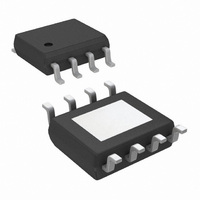
LM22675MRE-5.0/NOPB National Semiconductor, LM22675MRE-5.0/NOPB Datasheet - Page 11

LM22675MRE-5.0/NOPB
Manufacturer Part Number
LM22675MRE-5.0/NOPB
Description
IC REG SWITCH BUCK 1A 5V 8PSOP
Manufacturer
National Semiconductor
Series
SIMPLE SWITCHER®r
Type
Step-Down (Buck)r
Specifications of LM22675MRE-5.0/NOPB
Internal Switch(s)
Yes
Synchronous Rectifier
No
Number Of Outputs
1
Voltage - Output
5V
Current - Output
1A
Frequency - Switching
500kHz
Voltage - Input
4.5 ~ 42 V
Operating Temperature
-40°C ~ 125°C
Mounting Type
Surface Mount
Package / Case
8-PSOP
Dc To Dc Converter Type
Inverting/Step Down
Pin Count
8
Input Voltage
42V
Output Voltage
5V
Switching Freq
500kHz
Output Current
1A
Efficiency
90%
Package Type
PSOP EP
Output Type
Fixed
Switching Regulator
Yes
Mounting
Surface Mount
Input Voltage (min)
4.5V
Operating Temperature Classification
Automotive
Primary Input Voltage
12V
No. Of Outputs
1
No. Of Pins
8
Operating Temperature Range
-40°C To +125°C
Msl
MSL 3 - 168 Hours
Filter Terminals
SMD
Rohs Compliant
Yes
For Use With
551600236-001 - WEBENCH BUILD IT LM2267X 8-PSOP
Lead Free Status / RoHS Status
Lead free / RoHS Compliant
Power - Output
-
Lead Free Status / Rohs Status
Compliant
Other names
LM22675MRE-5.0TR
Available stocks
Company
Part Number
Manufacturer
Quantity
Price
Company:
Part Number:
LM22675MRE-5.0/NOPB
Manufacturer:
TI
Quantity:
5 241
Circuit Board Layout
Board layout is critical for switching power supplies. First, the
ground plane area must be sufficient for thermal dissipation
purposes. Second, appropriate guidelines must be followed
to reduce the effects of switching noise. Switch mode con-
verters are very fast switching devices. In such devices, the
rapid increase of input current combined with the parasitic
trace inductance generates unwanted L di/dt noise spikes.
The magnitude of this noise tends to increase as the output
current increases. This parasitic spike noise may turn into
electromagnetic interference (EMI) and can also cause prob-
lems in device performance. Therefore, care must be taken
in layout to minimize the effect of this switching noise.
The most important layout rule is to keep the AC current loops
as small as
converter. The top schematic shows a dotted line which rep-
resents the current flow during the FET switch on-state. The
middle schematic shows the current flow during the FET
switch off-state.
The bottom schematic shows the currents referred to as AC
currents. These AC currents are the most critical since current
is changing in very short time periods. The dotted lines of the
bottom schematic are the traces to keep as short as possible.
This will also yield a small loop area reducing the loop induc-
tance. To avoid functional problems due to layout, review the
PCB layout example. Best results are achieved if the place-
ment of the LM22675, the bypass capacitor, the Schottky
diode and the inductor are placed as shown in the example.
It is also recommended to use 2oz copper boards or thicker
to help thermal dissipation and to reduce the parasitic induc-
tances of board traces.
FIGURE 4. Current Flow in a Buck Application
possible.Figure 4
shows the current flow of a buck
30077024
11
Thermal Considerations
The two highest power dissipating components are the re-
circulating diode and the LM22675 regulator IC. The easiest
method to determine the power dissipation within the
LM22675 is to measure the total conversion losses (Pin –
Pout) then subtract the power losses in the Schottky diode
and output inductor. An approximation for the Schottky diode
loss is:
An approximation for the output inductor power is:
where R is the DC resistance of the inductor and the 1.1 factor
is an approximation for the AC losses. The regulator has an
exposed thermal pad to aid power dissipation. Adding several
vias under the device to the ground plane will greatly reduce
the regulator junction temperature. Selecting a diode with an
exposed pad will aid the power dissipation of the diode. The
most significant variables that affect the power dissipated by
the LM22675 are the output current, input voltage and oper-
ating frequency. The power dissipated while operating near
the maximum output current and maximum input voltage can
be appreciable. The junction-to-ambient thermal resistance of
the LM22675 will vary with the application. The most signifi-
cant variables are the area of copper in the PC board, the
number of vias under the IC exposed pad and the amount of
forced air cooling provided. The integrity of the solder con-
nection from the IC exposed pad to the PC board is critical.
Excessive voids will greatly diminish the thermal dissipation
capacity. The junction-to-ambient thermal resistance of the
LM22675 PSOP-8 package is specified in the electrical char-
acteristics table under the applicable conditions.
P = (1 - D) x I
P = I
OUT
2
x R x 1.1,
OUT
x V
D
www.national.com


