LM5007SD/NOPB National Semiconductor, LM5007SD/NOPB Datasheet - Page 3
LM5007SD/NOPB
Manufacturer Part Number
LM5007SD/NOPB
Description
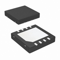
IC BUCK ADJ .5A 8LLP
Manufacturer
National Semiconductor
Type
Step-Down (Buck)r
Datasheet
1.LM5007SDNOPB.pdf
(12 pages)
Specifications of LM5007SD/NOPB
Internal Switch(s)
Yes
Synchronous Rectifier
No
Number Of Outputs
1
Voltage - Output
2.5 ~ 73 V
Current - Output
500mA
Frequency - Switching
800kHz
Voltage - Input
9 ~ 75 V
Operating Temperature
-40°C ~ 125°C
Mounting Type
Surface Mount
Package / Case
8-LLP
For Use With
LM5007SD-EVAL - EVALUATION BOARD FOR LM5007SDLM5007EVAL - EVALUATION BOARD FOR LM5007
Lead Free Status / RoHS Status
Lead free / RoHS Compliant
Power - Output
-
Other names
LM5007SD
LM5007SDTR
LM5007SDTR
Available stocks
Company
Part Number
Manufacturer
Quantity
Price
Company:

Part Number:
LM5007SD/NOPB
Manufacturer:
NS
Quantity:
693
Part Number:
LM5007SD/NOPB
Manufacturer:
TI/德州仪器
Quantity:
20 000


Pin Descriptions
Pin
1
2
3
4
5
6
7
8
-
Name
BST
RTN
R
Vcc
SW
R
Vin
FB
EP
ON
CL
Switching Node
Boost Boot–strap capacitor input
Current Limit OFF time programming pin
Toff = 10
Circuit Ground
Feedback Signal from Regulated Output
On time set pin
Ton = 1.42 x 10
Output from the internal high voltage bias regulator.
V
Input supply voltage
Exposed PAD, underside of the LLP package
option
CC
is nominally regulated to 7 Volts
-5
/ (0.59 + (FB / 7.22 x 10
-10
R
Description
ON
/ Vin
− 6
x R
3
CL
))
Power switching node. Connect to the LC output filter.
An external capacitor is required between the BST
and the SW pins. A 0.01uF ceramic capacitor is
recommended. An internal diode between Vcc and
BST completes the Buck gate drive bias network.
A resistor between this pin and RTN determines the
variation of off time, along with the FB pin voltage, per
cycle while in current limit. The off time is preset to
17uS if FB =0V and decreases as the FB pin voltage
increases.
This pin is connected to the inverting input of the
internal regulation comparator. The regulation
threshold is 2.5V.
A resistor between this pin and Vin sets the switch on
time as a function of Vin. The minimum recommended
on time is 300ns at the maximum input voltage.
If an auxiliary voltage is available to raise the voltage
on this pin, above the regulation setpoint (7V), the
internal series pass regulator will shutdown, reducing
the IC power dissipation. Do not exceed 14V. This
output provides gate drive power for the internal Buck
switch. An internal diode is provided between this pin
and the BST pin. A local 0.1uF decoupling capacitor
is recommended. Series pass regulator is current
limited to 10mA.
Recommended operating range: 9V to 75V.
Internally bonded to the die substrate. Connect to
GND potential for low thermal impedance.
Application Information
www.national.com
Related parts for LM5007SD/NOPB
Image
Part Number
Description
Manufacturer
Datasheet
Request
R

Part Number:
Description:
EVALUATION BOARD FOR LM5007SD
Manufacturer:
National Semiconductor
Datasheet:


Part Number:
Description:
National Semiconductor [8-Bit D/A Converter]
Manufacturer:
National Semiconductor
Datasheet:
Part Number:
Description:
National Semiconductor [Media Coprocessor]
Manufacturer:
National Semiconductor
Datasheet:
Part Number:
Description:
Digitally Controlled Tone and Volume Circuit with Stereo Audio Power Amplifier, Microphone Preamp Stage and National 3D Sound
Manufacturer:
National Semiconductor
Datasheet:
Part Number:
Description:
Digitally Controlled Tone and Volume Circuit with Stereo Audio Power Amplifier, Microphone Preamp Stage and National 3D Sound
Manufacturer:
National Semiconductor
Datasheet:
Part Number:
Description:
AC97 Rev 2 Codec with Sample Rate Conversion and National 3D Sound
Manufacturer:
National Semiconductor
Part Number:
Description:
Manufacturer:
National Semiconductor
Datasheet:
Part Number:
Description:
Manufacturer:
National Semiconductor
Datasheet:
Part Number:
Description:
General Purpose, Low Voltage, Low Power, Rail-to-Rail Output Operational Amplifiers
Manufacturer:
National Semiconductor
Datasheet:
Part Number:
Description:
8-bit 20 MSPS flash A/D converter.
Manufacturer:
National Semiconductor
Datasheet:
Part Number:
Description:
Low Noise Quad Operational Amplifier
Manufacturer:
National Semiconductor
Datasheet:
Part Number:
Description:
Quad Differential Line Receivers
Manufacturer:
National Semiconductor
Datasheet:
Part Number:
Description:
Quad High Speed Trapezoidal? Bus Transceiver
Manufacturer:
National Semiconductor
Datasheet: