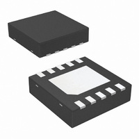
LM3678SD-1.2/NOPB National Semiconductor, LM3678SD-1.2/NOPB Datasheet - Page 11

LM3678SD-1.2/NOPB
Manufacturer Part Number
LM3678SD-1.2/NOPB
Description
IC CONV DC-DC STDN LV 1.5A 10LLP
Manufacturer
National Semiconductor
Series
PowerWise®r
Type
Step-Down (Buck)r
Datasheet
1.LM3678SD-1.2NOPB.pdf
(14 pages)
Specifications of LM3678SD-1.2/NOPB
Internal Switch(s)
Yes
Synchronous Rectifier
Yes
Number Of Outputs
1
Voltage - Output
0.8V, 1.2V
Current - Output
1.5A
Frequency - Switching
3.3MHz
Voltage - Input
2.5 ~ 5.5 V
Operating Temperature
-30°C ~ 85°C
Mounting Type
Surface Mount
Package / Case
10-LLP
For Use With
LM3678SD-1.2EV - BOARD EVAL FOR LM3678SD-1.2
Lead Free Status / RoHS Status
Lead free / RoHS Compliant
Power - Output
-
Other names
LM3678SD-1.2TR
Available stocks
Company
Part Number
Manufacturer
Quantity
Price
Company:
Part Number:
LM3678SD-1.2/NOPB
Manufacturer:
NS
Quantity:
6 734
Board Layout Considerations
PC board layout is an important part of DC-DC converter de-
sign. Poor board layout can disrupt the performance of a DC-
DC converter and surrounding circuitry by contributing to EMI,
ground bounce, and resistive voltage loss in the traces. These
can send erroneous signals to the DC-DC converter IC, re-
sulting in poor regulation or instability.
Good layout for the LM3678 can be implemented by following
a few simple design rules below.
1.
2.
3.
10µF for C
22µF for C
GRM21BR60J106K
Place the LM3678, inductor and filter capacitors close
together and make the traces short. The traces between
these components carry relatively high switching
currents and act as antennas. Following this rule reduces
radiated noise. Special care must be given to place the
input filter capacitor very close to the V
Arrange the components so that the switching current
loops curl in the same direction. During the first half of
each cycle, current flows from the input filter capacitor
through the LM3678 and inductor to the output filter
capacitor and back through ground, forming a current
loop. In the second half of each cycle, current is pulled
up from ground through the LM3678 by the inductor to
the output filter capacitor and then back through ground
forming a second current loop. Routing these loops so
the current curls in the same direction prevents magnetic
field reversal between the two half-cycles and reduces
radiated noise.
Connect the ground pins of the LM3678 and filter
capacitors together using generous component-side
copper fill as a pseudo-ground plane. Then, connect this
to the ground-plane (if one is used) with several vias. This
reduces ground-plane noise by preventing the switching
currents from circulating through the ground plane. It also
C2012X5R0J106K
JMK212BJ226MG
JMK212BJ106K
Model
IN
OUT
Ceramic, X5R
Ceramic, X5R
Ceramic, X5R
Ceramic, X5R
TABLE 2. Suggested Capacitors and Their Suppliers
Type
IN
and GND pin.
Taiyo-Yuden
Taiyo-Yuden
Vendor
Murata
TDK
11
4.
5.
6.
For detailed layout information, refer to Application Note 1722
LM3678 Evaluation Board.
In mobile phones, for example, a common practice is to place
the DC-DC converter on one corner of the board, arrange the
CMOS digital circuitry around it (since this also generates
noise), and then place sensitive preamplifiers and IF stages
on the diagonally opposing corner. Often, the sensitive cir-
cuitry is shielded with a metal pan and power to it is post-
regulated to reduce conducted noise, using low-dropout
linear regulators.
reduces ground bounce at the LM3678 by giving it a low-
impedance ground connection.
Use wide traces between the power components and for
power connections to the DC-DC converter circuit. This
reduces voltage errors caused by resistive losses across
the traces.
Route noise sensitive traces, such as the voltage
feedback path, away from noisy traces between the
power components. The voltage feedback trace must
remain close to the LM3678 circuit and should be direct
but should be routed opposite to noisy components. This
reduces EMI radiated onto the DC-DC converter’s own
voltage feedback trace. A good approach is to route the
feedback trace on another layer and to have a ground
plane between the top layer and layer on which the
feedback trace is routed. In the same manner for the
adjustable part it is desired to have the feedback dividers
on the bottom layer.
Place noise sensitive circuitry, such as radio IF blocks,
away from the DC-DC converter, CMOS digital blocks
and other noisy circuitry. Interference with noise-
sensitive circuitry in the system can be reduced through
distance.
Voltage Rating
6.3V
6.3V
6.3V
6.3V
0805 (2012)
0805 (2012)
0805 (2012)
0805 (2012)
Inch (mm)
Case Size
www.national.com


