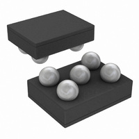
LM3673TL-1.5/NOPB National Semiconductor, LM3673TL-1.5/NOPB Datasheet - Page 13

LM3673TL-1.5/NOPB
Manufacturer Part Number
LM3673TL-1.5/NOPB
Description
IC CONV DC/DC 350MA 1.5V 5MICRO
Manufacturer
National Semiconductor
Series
PowerWise®r
Type
Step-Down (Buck)r
Datasheet
1.LM3673TL-1.5NOPB.pdf
(20 pages)
Specifications of LM3673TL-1.5/NOPB
Internal Switch(s)
Yes
Synchronous Rectifier
Yes
Number Of Outputs
1
Voltage - Output
1.5V
Current - Output
350mA
Frequency - Switching
2MHz
Voltage - Input
2.7 ~ 5.5 V
Operating Temperature
-30°C ~ 85°C
Mounting Type
Surface Mount
Package / Case
5-MicroSMD
Power - Output
1.18W
For Use With
LM3673TL-1.5EV - BOARD EVALUATION LM3673TL-1.5
Lead Free Status / RoHS Status
Lead free / RoHS Compliant
Other names
LM3673TL-1.5TR
Available stocks
Company
Part Number
Manufacturer
Quantity
Price
SHUTDOWN MODE
Setting the EN input pin low (<0.4V) places the LM3673 in
shutdown mode. During shutdown the PFET switch, NFET
switch, reference, control and bias circuitry of the LM3673 are
turned off. Setting EN high (>1.0V) enables normal operation.
It is recommended to set EN pin low to turn off the LM3673
during system power up and undervoltage conditions when
the supply is less than 2.7V. Do not leave the EN pin floating.
SOFT START
The LM3673 has a soft-start circuit that limits in-rush current
during start-up. During start-up the switch current limit is in-
creased in steps. Soft start is activated only if EN goes from
logic low to logic high after Vin reaches 2.7V. Soft start is im-
plemented by increasing switch current limit in steps of 70mA,
140mA, 280mA and 750mA (typical switch current limit). The
start-up time thereby depends on the output capacitor and
load current. Typical start-up times with a 10µF output ca-
pacitor and 150mA load is 280µs and with 5mA load is 240µs.
LDO - LOW DROP OUT OPERATION
The LM3673-ADJ can operate at 100% duty cycle (no switch-
ing; PMOS switch completely on) for low drop out support of
the output voltage. In this way the output voltage will be con-
trolled down to the lowest possible input voltage. When the
device operates near 100% duty cycle, output voltage ripple
is approximately 25mV.
The minimum input voltage needed to support the output volt-
age is
V
Application Information
OUTPUT VOLTAGE SELECTION FOR LM3673-ADJ
The output voltage of the adjustable parts can be pro-
grammed through the resistor network connected from V
to FB, then to GND. V
FB equal to 0.5V. The resistor from FB to GND (R2) should
be 200 kΩ to keep the current drawn through this network well
IN, MIN
• I
• R
• R
LOAD
DSON, PFET
INDUCTOR
= I
LOAD
* (R
DSON, PFET
OUT
Load current
Drain to source resistance of PFET
switch in the triode region
Inductor resistance
is adjusted to make the voltage at
+ R
INDUCTOR
) + V
OUT
OUT
13
below the 16 µA quiescent current level (PFM mode) but large
enough that it is not susceptible to noise. If R2 is 200 kΩ, and
V
will be 2.5 µA. The output voltage of the adjustable parts
ranges from 1.1V to 3.3V.
The formula for output voltage selection is:
•
•
•
•
For any output voltage greater than or equal to 1.1V, a zero
must be added around 45 kHz for stability. The formula for
calculation of C1 is:
For output voltages higher than 2.5V, a pole must be placed
at 45 kHz as well. If the pole and zero are at the same fre-
quency the formula for calculation of C2 is:
The formula for location of zero and pole frequency created
by adding C1 and C2 is given below. By adding C1, a zero as
well as a higher frequency pole is introduced.
See the "LM3673-ADJ configurations for various V
FB
V
V
R1: feedback resistor from V
R2: feedback resistor from FB to GND
is 0.5V, the current through the resistor feedback network
OUT
FB
: feedback voltage = 0.5V
: output voltage (volts)
OUT
to FB
www.national.com
OUT
" table.


