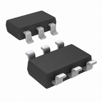
LM2736XMK/NOPB National Semiconductor, LM2736XMK/NOPB Datasheet - Page 7

LM2736XMK/NOPB
Manufacturer Part Number
LM2736XMK/NOPB
Description
IC REG PWM STPDWN 750MA TSOT23-6
Manufacturer
National Semiconductor
Type
Step-Down (Buck)r
Datasheet
1.LM2736YMKNOPB.pdf
(22 pages)
Specifications of LM2736XMK/NOPB
Internal Switch(s)
Yes
Synchronous Rectifier
No
Number Of Outputs
1
Voltage - Output
1.25 ~ 16 V
Current - Output
750mA
Frequency - Switching
1.6MHz
Voltage - Input
3 ~ 18 V
Operating Temperature
-40°C ~ 125°C
Mounting Type
Surface Mount
Package / Case
TSOT-23-6, TSOT-6
For Use With
LM2736X EVAL - BOARD EVALUATION LM2736X
Lead Free Status / RoHS Status
Lead free / RoHS Compliant
Power - Output
-
Other names
LM2736XMK
LM2736XMKTR
LM2736XMKTR
Available stocks
Company
Part Number
Manufacturer
Quantity
Price
Company:
Part Number:
LM2736XMK/NOPB
Manufacturer:
SKYWORKS
Quantity:
12 000
Part Number:
LM2736XMK/NOPB
Manufacturer:
TI/德州仪器
Quantity:
20 000
Block Diagram
Application Information
THEORY OF OPERATION
The LM2736 is a constant frequency PWM buck regulator IC
that delivers a 750mA load current. The regulator has a
preset switching frequency of either 550kHz (LM2736Y) or
1.6MHz (LM2736X). These high frequencies allow the
LM2736 to operate with small surface mount capacitors and
inductors, resulting in DC/DC converters that require a mini-
mum amount of board space. The LM2736 is internally
compensated, so it is simple to use, and requires few exter-
nal components. The LM2736 uses current-mode control to
regulate the output voltage.
The following operating description of the LM2736 will refer
to the Simplified Block Diagram (Figure 1) and to the wave-
forms in Figure 2. The LM2736 supplies a regulated output
voltage by switching the internal NMOS control switch at
constant frequency and variable duty cycle. A switching
cycle begins at the falling edge of the reset pulse generated
by the internal oscillator. When this pulse goes low, the
output control logic turns on the internal NMOS control
switch. During this on-time, the SW pin voltage (V
up to approximately V
creases with a linear slope. I
sense amplifier, which generates an output proportional to
the switch current. The sense signal is summed with the
regulator’s corrective ramp and compared to the error am-
plifier’s output, which is proportional to the difference be-
tween the feedback voltage and V
comparator output goes high, the output switch turns off until
the next switching cycle begins. During the switch off-time,
inductor current discharges through Schottky diode D1,
which forces the SW pin to swing below ground by the
IN
, and the inductor current (I
L
is measured by the current-
REF
. When the PWM
SW
) swings
L
) in-
FIGURE 1.
7
forward voltage (V
adjusts the duty cycle (D) to maintain a constant output
voltage.
BOOST FUNCTION
Capacitor C
generate a voltage V
voltage to the internal NMOS control switch. To properly
drive the internal NMOS switch during its on-time, V
needs to be at least 1.6V greater than V
LM2736 will operate with this minimum voltage, it may not
have sufficient gate drive to supply large values of output
FIGURE 2. LM2736 Waveforms of SW Pin Voltage and
BOOST
D
and diode D2 in Figure 3 are used to
) of the catch diode. The regulator loop
Inductor Current
BOOST
. V
BOOST
- V
SW
SW
is the gate drive
. Although the
20124206
20124207
www.national.com
BOOST


