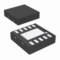
LM2750LD-ADJ/NOPB National Semiconductor, LM2750LD-ADJ/NOPB Datasheet - Page 9

LM2750LD-ADJ/NOPB
Manufacturer Part Number
LM2750LD-ADJ/NOPB
Description
IC CONV REG SW CAP ADJ 10-LLP
Manufacturer
National Semiconductor
Type
Step-Up (Boost), Switched Capacitor (Charge Pump), Doublerr
Datasheet
1.LM2750LD-ADJNOPB.pdf
(16 pages)
Specifications of LM2750LD-ADJ/NOPB
Internal Switch(s)
Yes
Synchronous Rectifier
No
Number Of Outputs
1
Voltage - Output
3.8 ~ 5.2 V
Current - Output
120mA
Frequency - Switching
1.7MHz
Voltage - Input
2.7 ~ 5.6 V
Operating Temperature
-40°C ~ 85°C
Mounting Type
Surface Mount
Package / Case
10-LLP
For Use With
LM2750LD-ADJEV - BOARD EVAL LM2750LD-ADJ
Lead Free Status / RoHS Status
Lead free / RoHS Compliant
Power - Output
-
Other names
LM2750LD-ADJ
LM2750LD-ADJTR
LM2750LD-ADJTR
Available stocks
Company
Part Number
Manufacturer
Quantity
Price
Company:
Part Number:
LM2750LD-ADJ/NOPB
Manufacturer:
FSC
Quantity:
6 000
Part Number:
LM2750LD-ADJ/NOPB
Manufacturer:
TI/德州仪器
Quantity:
20 000
Operation Description
increases to the point that there is zero voltage drop across
the regulator, V’ equals the input voltage, and the output
voltage is "on the edge" of regulation. Additional output
current causes the output voltage to fall out of regulation,
and the LM2750 operation is similar to a basic open-loop
doubler. As in a voltage doubler, increase in output current
results in output voltage drop proportional to the output
resistance of the doubler. The out-of-regulation LM2750 out-
put voltage can be approximated by:
Again, this equation only applies at low input voltage and
high output current where the LM2750 is not regulating. See
Output Current vs. Output Voltage curves in the Typical
Performance Characteristics section for more details.
A more complete calculation of output resistance takes into
account the effects of switching frequency, flying capaci-
tance, and capacitor equivalent series resistance (ESR).
This equation is shown below:
Switch resistance (5Ω typ.) dominates the output resistance
equation of the LM2750. With a 1.7MHz typical switching
frequency, the 1/(FxC) component of the output resistance
contributes only 0.6Ω to the total output resistance. Increas-
ing the flying capacitance will only provide minimal improve-
ment to the total output current capability of the LM2750. In
some applications it may be desirable to reduce the value of
the flying capacitor below 1µF to reduce solution size and/or
cost, but this should be done with care so that output resis-
tance does not increase to the point that undesired output
voltage droop results. If ceramic capacitors are used, ESR
will be a negligible factor in the total output resistance, as the
ESR of quality ceramic capacitors is typically much less than
100mΩ.
THERMAL SHUTDOWN
The LM2750 implements a thermal shutdown mechanism to
protect the device from damage due to overheating. When
the junction temperature rises to 150
FIGURE 1. LM2750 Output Resistance Model
V
OUT
= 2xV
IN
- I
OUT
x R
(Continued)
OUT
o
C (typ.), the part
20035109
9
switches into shutdown mode. The LM2750 releases thermal
shutdown when the junction temperature of the part is re-
duced to 130
Thermal shutdown is most-often triggered by self-heating,
which occurs when there is excessive power dissipation in
the device and/or insufficient thermal dissipation. LM2750
power dissipation increases with increased output current
and input voltage (see Power Efficiency and Power Dissi-
pation section). When self-heating brings on thermal shut-
down, thermal cycling is the typical result. Thermal cycling is
the repeating process where the part self-heats, enters ther-
mal shutdown (where internal power dissipation is practically
zero), cools, turns-on, and then heats up again to the ther-
mal shutdown threshold. Thermal cycling is recognized by a
pulsing output voltage and can be stopped be reducing the
internal power dissipation (reduce input voltage and/or out-
put current) or the ambient temperature. If thermal cycling
occurs under desired operating conditions, thermal dissipa-
tion performance must be improved to accommodate the
power dissipation of the LM2750. Fortunately, the LLP pack-
age has excellent thermal properties that, when soldered to
a PCB designed to aid thermal dissipation, allows the
LM2750 to operate under very demanding power dissipation
conditions.
OUTPUT CURRENT LIMITING
The LM2750 contains current limit circuitry that protects the
device in the event of excessive output current and/or output
shorts to ground. Current is limited to 300mA (typ.) when the
output is shorted directly to ground. When the LM2750 is
current limiting, power dissipation in the device is likely to be
quite high. In this event, thermal cycling should be expected
(see Thermal Shutdown section).
PROGRAMMING THE OUTPUT VOLTAGE OF THE
LM2750-ADJ
As shown in the application circuit of Figure 2, the output
voltage of the LM2750-ADJ can be programmed with a
simple resistor divider (see resistors R1 and R2). The values
of the feedback resistors set the output voltage, as deter-
mined by the following equation:
In the equation above, the "1.23V" term is the nominal
voltage of the feedback pin when the feedback loop is cor-
rectly established and the part is operating normally. The
sum of the resistance of the two feedback resistors should
be between 15kΩ and 20kΩ:
If larger feedback resistors are desired, a 10pF capacitor
should be placed in parallel with resistor R1.
V
15kΩ
OUT
= 1.23V x (1 + R1/ R2)
<
o
(R1 + R2)
C (typ.).
<
20kΩ
www.national.com


