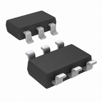
LM2736YMK National Semiconductor, LM2736YMK Datasheet - Page 11

LM2736YMK
Manufacturer Part Number
LM2736YMK
Description
IC REG PWM STPDWN 750MA TSOT23-6
Manufacturer
National Semiconductor
Type
Step-Down (Buck)r
Datasheet
1.LM2736YMKNOPB.pdf
(22 pages)
Specifications of LM2736YMK
Internal Switch(s)
Yes
Synchronous Rectifier
No
Number Of Outputs
1
Voltage - Output
1.25 ~ 16 V
Current - Output
750mA
Frequency - Switching
550kHz
Voltage - Input
3 ~ 18 V
Operating Temperature
-40°C ~ 125°C
Mounting Type
Surface Mount
Package / Case
TSOT-23-6, TSOT-6
Leaded Process Compatible
No
Rohs Compliant
No
Peak Reflow Compatible (260 C)
No
For Use With
LM2736Y EVAL - BOARD EVALUATION LM2736Y
Lead Free Status / RoHS Status
Lead free / RoHS Compliant
Power - Output
-
Other names
*LM2736YMK
*LM2736YMK/NOPB
LM2736YMKCT
*LM2736YMK/NOPB
LM2736YMKCT
Available stocks
Company
Part Number
Manufacturer
Quantity
Price
Part Number:
LM2736YMK
Manufacturer:
TI/德州仪器
Quantity:
20 000
Company:
Part Number:
LM2736YMK/NOPB
Manufacturer:
TI
Quantity:
11 670
Company:
Part Number:
LM2736YMKX
Manufacturer:
NSC
Quantity:
1 450
Company:
Part Number:
LM2736YMKX
Manufacturer:
MIC
Quantity:
20
Part Number:
LM2736YMKX
Manufacturer:
NS/国半
Quantity:
20 000
Company:
Part Number:
LM2736YMKX/NOPB
Manufacturer:
TI
Quantity:
11 670
Part Number:
LM2736YMKX/NOPB
Manufacturer:
TI/德州仪器
Quantity:
20 000
Design Guide
OUTPUT VOLTAGE
The output voltage is set using the following equation where
R2 is connected between the FB pin and GND, and R1 is
connected between V
is 10kΩ.
PCB Layout Considerations
When planning layout there are a few things to consider
when trying to achieve a clean, regulated output. The most
important consideration when completing the layout is the
close coupling of the GND connections of the C
and the catch diode D1. These ground ends should be close
to one another and be connected to the GND plane with at
least two through-holes. Place these components as close to
the IC as possible. Next in importance is the location of the
O
and the FB pin. A good value for R2
(Continued)
IN
capacitor
11
GND connection of the C
near the GND connections of C
There should be a continuous ground plane on the bottom
layer of a two-layer board except under the switching node
island.
The FB pin is a high impedance node and care should be
taken to make the FB trace short to avoid noise pickup and
inaccurate regulation. The feedback resistors should be
placed as close as possible to the IC, with the GND of R2
placed as close as possible to the GND of the IC. The V
trace to R1 should be routed away from the inductor and any
other traces that are switching.
High AC currents flow through the V
so they should be as short and wide as possible. However,
making the traces wide increases radiated noise, so the
designer must make this trade-off. Radiated noise can be
decreased by choosing a shielded inductor.
The remaining components should also be placed as close
as possible to the IC. Please see Application Note AN-1229
for further considerations and the LM2736 demo board as an
example of a four-layer layout.
OUT
capacitor, which should be
IN
and D1.
IN
, SW and V
www.national.com
OUT
traces,
OUT


