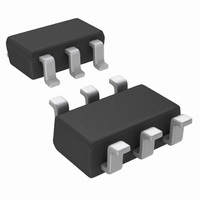
LM2664M6/NOPB National Semiconductor, LM2664M6/NOPB Datasheet - Page 2

LM2664M6/NOPB
Manufacturer Part Number
LM2664M6/NOPB
Description
IC SW CAP/INV ADJ 40MA SOT23-6
Manufacturer
National Semiconductor
Type
Switched Capacitor (Charge Pump), Invertingr
Datasheet
1.LM2664M6NOPB.pdf
(9 pages)
Specifications of LM2664M6/NOPB
Internal Switch(s)
Yes
Synchronous Rectifier
No
Number Of Outputs
1
Voltage - Output
-1.8 ~ -5.5 V
Current - Output
40mA
Frequency - Switching
160kHz
Voltage - Input
1.8 ~ 5.5 V
Operating Temperature
-40°C ~ 85°C
Mounting Type
Surface Mount
Package / Case
SOT-23-6
Power - Output
600mW
Primary Input Voltage
5V
No. Of Outputs
1
Output Voltage
-5.5V
Output Current
40mA
No. Of Pins
6
Operating Temperature Range
-40°C To +85°C
Msl
MSL 1 - Unlimited
Filter Terminals
SMD
Rohs Compliant
Yes
Lead Free Status / RoHS Status
Lead free / RoHS Compliant
Other names
LM2664M6
LM2664M6TR
LM2664M6TR
Available stocks
Company
Part Number
Manufacturer
Quantity
Price
Company:
Part Number:
LM2664M6/NOPB
Manufacturer:
SAMSUNG
Quantity:
3 400
www.national.com
V+
I
I
V
I
R
R
f
f
P
V
Q
SD
L
OSC
SW
SD
EFF
OEFF
SW
OUT
Absolute Maximum Ratings
If Military/Aerospace specified devices are required,
please contact the National Semiconductor Sales Office/
Distributors for availability and specifications.
Electrical Characteristics
Limits in standard typeface are for T
less otherwise specified: V+ = 5V, C
Note 1: Absolute maximum ratings indicate limits beyond which damage to the device may occur. Electrical specifications do not apply when operating the device
beyond its rated operating conditions.
Note 2: OUT may be shorted to GND for one second without damage. However, shorting OUT to V+ may damage the device and should be avoided. Also, for
temperatures above 85˚C, OUT must not be shorted to GND or V+, or device may be damaged.
Note 3: The maximum allowable power dissipation is calculated by using P
ambient temperature, and θ
Note 4: In the test circuit, capacitors C
output voltage and efficiency.
Note 5: Min. and Max. limits are guaranteed by design, test, or statistical analysis.
Note 6: Typical numbers are not guaranteed but represent the most likely norm.
Note 7: The minimum input high for the shutdown pin equals 40% of V+.
Note 8: The maximum input low for the shutdown pin equals 20% of V+.
Note 9: Specified output resistance includes internal switch resistance and capacitor ESR. See the details in the application information for simple negative voltage
converter.
Note 10: The output switches operate at one half of the oscillator frequency, f
Symbol
Supply Voltage (V+ to GND, or GND to OUT)
SD
V+ and OUT Continuous Output Current
Output Short-Circuit Duration to GND (Note 2)
Continuous Power
Dissipation (T
Supply Voltage
Supply Current
Shutdown Supply Current
Shutdown Pin Input Voltage
Output Current
Sum of the R
internal MOSFET switches
Output Resistance (Note 9)
Oscillator Frequency
Switching Frequency
Power Efficiency
Voltage Conversion Efficiency
A
= 25˚C)(Note 3)
JA
Parameter
is the junction-to-ambient thermal resistance of the specified package.
ds(on)
of the four
1
and C
(GND − 0.3V) to (V+ +
J
1
2
= 25˚C, and limits in boldface type apply over the full operating temperature range. Un-
= C
are 3.3 µF, 0.3Ω maximum ESR capacitors. Capacitors with higher ESR will increase output resistance, reduce
2
= 3.3 µF. (Note 4)
(Note 1)
Condition
No Load
Normal Operation
Shutdown Mode
I
I
(Note 10)
(Note 10)
R
OUT
I
No Load
L
L
L
L
600 mW
= 40 mA
= 40 mA
= 40 mA to GND
(1.0k) between GND and
50 mA
1 sec.
0.3V)
5.8V
DMax
OSC
2
= (T
= 2f
JMax
T
θ
Operating Junction
Temperature Range
Storage Temperature Range
Lead Temp. (Soldering, 10 seconds)
ESD Rating
SW
JA
JMax
.
− T
(Note 3)
(Note 3)
A
)/θ
JA
, where T
(Note 5)
(Note 7)
JMax
Min
1.8
2.0
40
80
40
90
99
is the maximum junction temperature, T
(Note 6)
99.96
Typ
220
160
12
80
94
91
1
4
−65˚C to +150˚C
(Note 5)
(Note 8)
Max
500
5.5
0.8
25
8
−40˚ to 85˚C
210˚C/W
150˚C
300˚C
A
Units
2kV
is the
kHz
kHz
mA
µA
µA
Ω
Ω
%
%
V
V


