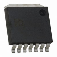
MIC4685WR Micrel Inc, MIC4685WR Datasheet - Page 3

MIC4685WR
Manufacturer Part Number
MIC4685WR
Description
IC REG BUCK 3A ADJ VOLT HE 7SPAK
Manufacturer
Micrel Inc
Series
SuperSwitcher™r
Type
Step-Down (Buck)r
Datasheet
1.MIC4685WR_TR.pdf
(17 pages)
Specifications of MIC4685WR
Internal Switch(s)
Yes
Synchronous Rectifier
No
Number Of Outputs
1
Voltage - Output
Adj to 1.235V
Current - Output
3A
Frequency - Switching
200kHz
Voltage - Input
4 ~ 30 V
Operating Temperature
-40°C ~ 125°C
Mounting Type
Surface Mount
Package / Case
SPak-7
Power - Output
1.14W
Lead Free Status / RoHS Status
Lead free / RoHS Compliant
Other names
576-1224
Available stocks
Company
Part Number
Manufacturer
Quantity
Price
Company:
Part Number:
MIC4685WR
Manufacturer:
MICREL
Quantity:
79
Part Number:
MIC4685WR
Manufacturer:
MICREL/麦瑞
Quantity:
20 000
Company:
Part Number:
MIC4685WRTR
Manufacturer:
MICREL
Quantity:
1 446
Detailed Pin Description
Switch (SW, Pin 6)
The switch pin is tied to the emitter of the main internal
NPN transistor. This pin is biased up to the input voltage,
minus the V
emitter is also driven negative when the output inductor’s
magnetic field collapses at turn-off. During the OFF time,
the SW pin is clamped by the output Schottky diode
typically to a –0.5V.
Ground (GND, Pin 4, Tab)
There are two main areas of concern when it comes to the
ground pin, EMI and ground current. In a buck regulator or
any other non-isolated switching regulator, the output
capacitor(s) and diode(s) ground is referenced back to the
switching regulator’s or controller’s ground pin. Any
resistance between these reference points causes an
offset voltage/IR drop proportional to load current and poor
load regulation. This is why it’s important to keep the
output grounds placed as close as possible to the
switching regulator’s ground pin. To keep radiated EMI to
a minimum, it is necessary to place the input capacitor
ground lead as close as possible to the switching
regulator’s ground pin.
Input Voltage (V
The V
This pin is also connected to the internal regulator. The
output diode or clamping diode should have its cathode as
close as possible to this point to avoid voltage spikes
adding to the voltage across the collector.
Micrel, Inc.
January 2010
IN
pin is the collector of the main NPN pass element.
SAT
, of the main NPN pass element. The
IN
, Pin 2)
3
Bootstrap (BS, Pin 1)
The bootstrap pin, in conjunction with the external
bootstrap capacitor, provides a bias voltage higher than
the input voltage to the MIC4685’s main NPN pass
element. The bootstrap capacitor sees the dv/dt of the
switching action at the SW pin as an AC voltage. The
bootstrap capacitor then couples the AC voltage back to
the BS pin, plus the dc offset of V
used to provide additional drive to the main switch; in this
case, a NPN transistor.
This additional drive reduces the NPN’s saturation voltage
and increases efficiency, from a V
efficiency to a V
respectively.
Feedback (FB, Pin 3)
The feedback pin is tied to the inverting side of an error
amplifier. The noninverting side is tied to a 1.235V
bandgap reference. An external resistor voltage divider is
required from the output-to-ground, with the center tied to
the feedback pin. See Tables 1 and 2 for recommended
resistor values.
Enable (EN, Pin 5)
The enable (EN) input is used to turn on the regulator and
is TTL compatible. Note: connect the enable pin to the
input if unused. A logic-high enables the regulator. A logic-
low shuts down the regulator and reduces the stand-by
quiescent input current to typically 150µA. The enable pin
has an up-per threshold of 2.0V minimum and lower
threshold of 0.8V maximum. The hysterisis provided by the
upper and lower thresholds acts as an UVLO and prevents
unwanted turn on of the regulator due to noise.
SAT
of 0.5V and 88% efficiency
IN
where it is rectified and
SAT
of 1.8V, and 75%
M9999-012610
MIC4685


