IR3841WMTR1PBF International Rectifier, IR3841WMTR1PBF Datasheet - Page 12
IR3841WMTR1PBF
Manufacturer Part Number
IR3841WMTR1PBF
Description
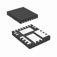
IC REG SYNC BUCK 8A 15-QFN
Manufacturer
International Rectifier
Series
SupIRBuck™r
Type
Step-Down (Buck)r
Datasheet
1.IR3841WMTR1PBF.pdf
(34 pages)
Specifications of IR3841WMTR1PBF
Internal Switch(s)
Yes
Synchronous Rectifier
Yes
Number Of Outputs
1
Voltage - Output
0.7 ~ 14.4 V
Current - Output
8A
Frequency - Switching
225kHz ~ 1.65MHz
Voltage - Input
1.5 ~ 16 V
Operating Temperature
-40°C ~ 125°C
Mounting Type
Surface Mount
Package / Case
15-PowerVQFN
Power - Output
1.5W
Primary Input Voltage
16V
No. Of Outputs
1
Output Voltage
14.4V
Output Current
8A
No. Of Pins
15
Operating Temperature Range
-40°C To +125°C
Output Voltage Adjustable Max, Vout
14.4V
Rohs Compliant
Yes
Part Status
Preferred
Package
PQFN / 5 x 6
Circuit
Single Output
Iout (a)
8
Switch Freq (khz)
250 - 1500
Input Range (v)
1.5 - 16
Output Range (v)
0.7 - 0.9*Vin
Ocp Otp Uvlo Pre-bias Soft Start And
PGOOD + EN + SEQ + OVD
Design Tool
Yes
Server Storage
Yes
Routers Switches
Yes
Base Station Telecom
Yes
Lead Free Status / RoHS Status
Lead free / RoHS Compliant
Other names
IR3841WMTR1PBFTR


Circuit Description
THEORY OF OPERATION
Introduction
The IR3841W uses a PWM voltage mode control
scheme with external compensation to provide
good noise immunity and maximum flexibility in
selecting inductor values and capacitor types.
The switching frequency is programmable from
250kHz to 1.5MHz and provides the capability of
optimizing the design in terms of size and
performance.
IR3841W provides precisely regulated output
voltage programmed via two external resistors
from 0.7V to 0.9*Vin.
The IR3841W operates with an external bias
supply from 4.5V to 5.5V, allowing an extended
operating input voltage range from 1.5V to 16V.
The device utilizes the on-resistance of the low
side MOSFET as current sense element, this
method enhances the converter’s efficiency and
reduces cost by eliminating the need for external
current sense resistor
IR3841W includes two low R
using IR’s HEXFET technology. These are
specifically
applications.
Under-Voltage Lockout and POR
The under-voltage lockout circuit monitors the
input supply Vcc and the Enable input. It assures
that the MOSFET driver outputs remain in the off
state whenever either of these two signals drop
below the set thresholds. Normal operation
resumes once Vcc and Enable rise above their
thresholds.
The POR (Power On Ready) signal is generated
when all these signals reach the valid logic level
(see system block diagram). When the POR is
asserted the soft start sequence starts (see soft
start section).
Enable
The Enable features another level of flexibility for
start up. The Enable has precise threshold which
is internally monitored by Under-Voltage Lockout
(UVLO) circuit. Therefore, the IR3841W will turn
on only when the voltage at the Enable pin
exceeds this threshold, typically, 1.2V.
Rev 5.0
designed
.
for
high
ds(on)
MOSFETs
efficiency
If the input to the Enable pin is derived from the
bus voltage by a suitably programmed resistive
divider, it can be ensured that the IR3841W does
not turn on until the bus voltage reaches the
desired level. Only after the bus voltage reaches
or exceeds this level will the voltage at Enable
pin exceed its threshold, thus enabling the
IR3841W. Therefore, in addition to being a logic
input pin to enable the IR3841W, the Enable
feature, with its precise threshold, also allows the
user to implement an Under-Voltage Lockout for
the bus voltage V
for high output voltage applications, where we
might want the IR3841W to be disabled at least
until V
Figure 3b. shows the recommended start-up
sequence for the non-sequenced operation of
IR3841W, when Enable is used as a logic input.
Fig. 3b. Recommended startup sequence,
Fig. 3a. Normal Start up, Device turns on
in
when the Bus voltage reaches 10.2V
exceeds the desired output voltage level.
Non-Sequenced operation
in
IR3841WMPbF
. This is desirable particularly
12
Related parts for IR3841WMTR1PBF
Image
Part Number
Description
Manufacturer
Datasheet
Request
R

Part Number:
Description:
Integrated 8a Synchronous Buck Regulator
Manufacturer:
International Rectifier Corp.
Datasheet:
Part Number:
Description:
SCHOTTKY RECTIFIER
Manufacturer:
International Rectifier Corp.
Datasheet:
Part Number:
Description:
SCHOTTKY RECTIFIER
Manufacturer:
International Rectifier Corp.
Datasheet:
Part Number:
Description:
SCHOTTKY RECTIFIER
Manufacturer:
International Rectifier Corp.
Datasheet:
Part Number:
Description:
SCHOTTKY RECTIFIER
Manufacturer:
International Rectifier Corp.
Datasheet:
Part Number:
Description:
SCHOTTKY RECTIFIER
Manufacturer:
International Rectifier Corp.
Datasheet:
Part Number:
Description:
SCHOTTKY RECTIFIER
Manufacturer:
International Rectifier Corp.
Datasheet:
Part Number:
Description:
SCHOTTKY RECTIFIER
Manufacturer:
International Rectifier Corp.
Datasheet:
Part Number:
Description:
SCHOTTKY RECTIFIER
Manufacturer:
International Rectifier Corp.
Datasheet:
Part Number:
Description:
SCHOTTKY RECTIFIER
Manufacturer:
International Rectifier Corp.
Datasheet:
Part Number:
Description:
SCHOTTKY RECTIFIER
Manufacturer:
International Rectifier Corp.
Datasheet:
Part Number:
Description:
SCHOTTKY RECTIFIER
Manufacturer:
International Rectifier Corp.
Datasheet:
Part Number:
Description:
SCHOTTKY RECTIFIER
Manufacturer:
International Rectifier Corp.
Datasheet:
Part Number:
Description:
SCHOTTKY RECTIFIER
Manufacturer:
International Rectifier Corp.
Datasheet:
Part Number:
Description:
SCHOTTKY RECTIFIER
Manufacturer:
International Rectifier Corp.
Datasheet: