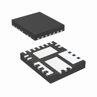
IR3840MTR1PBF International Rectifier, IR3840MTR1PBF Datasheet - Page 14

IR3840MTR1PBF
Manufacturer Part Number
IR3840MTR1PBF
Description
IC REG SYNC SUPIRBUCK 12A 5X6QFN
Manufacturer
International Rectifier
Series
SupIRBuck™r
Type
Step-Down (Buck)r
Datasheet
1.IR3840MTR1PBF.pdf
(32 pages)
Specifications of IR3840MTR1PBF
Internal Switch(s)
Yes
Synchronous Rectifier
Yes
Number Of Outputs
1
Voltage - Output
0.7 ~ 14.4 V
Current - Output
12A
Frequency - Switching
250kHz ~ 1.5MHz
Voltage - Input
1.5 ~ 16 V
Operating Temperature
-40°C ~ 125°C
Mounting Type
Surface Mount
Package / Case
15-PowerVQFN
Power - Output
2.6W
Part Status
Active
Package
PQFN / 5 x 6
Circuit
Single Output
Iout (a)
12
Switch Freq (khz)
250 - 1500
Input Range (v)
1.5 - 16
Output Range (v)
0.7 - 0.9*Vin
Ocp Otp Uvlo Pre-bias Soft Start And
PGOOD + EN + SEQ
Server Storage
Yes
Routers Switches
Yes
Base Station Telecom
Yes
Lead Free Status / RoHS Status
Lead free / RoHS Compliant
Other names
IR3840MTR1PBFTR
Thermal Shutdown
Temperature sensing is provided inside IR3840.
The trip threshold is typically set to 140
trip threshold is exceeded, thermal shutdown
turns off both MOSFETs and discharges the soft
start capacitor.
Automatic restart is initiated when the sensed
temperature drops within the operating range.
There is a 20
shutdown threshold.
Output Voltage Sequencing
The
programmable sequencing options using Seq,
Enable and Power Good pins.
Fig. 8a. Simultaneous Power-up of the slave
06/18/09
Through these pins, voltage sequencing such as
simultaneous
implemented. Figure 8. shows simultaneous
sequencing
power-up, the voltage at the Seq pin of the slave
reaches 0.7V before the Fb pin of the master. For
R
the slave follows that of the master until the
voltage at the Seq pin of the slave reaches 0.7 V.
After the voltage at the Seq pin of the slave
exceeds 0.85V, the internal 0.7V reference of
the slave dictates its output voltage.
E
/R
F
IR3840
with respect to the master.
=R
C
/R
Simultaneous Powerup
D
configurations.
o
, therefore, the output voltage of
C hysteresis in the thermal
can
and
accommodate
sequential
Vo1
Vo2
In
simultaneous
o
C. When
can
user
be
RE
RF
1.5V <Vin<16V
Vo(master)
PGood
4.5V <Vcc<5.5V
1.5V <Vin<16V
4.5V <Vcc<5.5V
Power Good Output
The IC continually monitors the output voltage via
Feedback (Fb pin). The feedback voltage is
compared to a fixed voltage. As soon as the Fb
voltage reaches 0.88*V
flags. This pin is open drain and it needs to be
externally pulled high. High state indicates that
output is in regulation. Fig 9. shows the timing
diagram for the PGood function.
PGood
Fig. 8b. Application Circuit for Simultaneous
Seq
Vcc
Rt
SS/ SD
PGood
Seq
Vcc
Rt
SS/ SD
PGood
Sequencing
Enable
Gnd
Enable
Gnd
Vin
IR3840MPbF
PGnd
Vin
PGnd
OCSet
ref
Comp
Boot
OCSet
SW
Comp
Fb
, the Power Good signal
Boot
SW
Fb
RA
RC
RB
RD
14
Vo(master)
Vo(slave)


