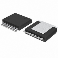
BD9007HFP-TR Rohm Semiconductor, BD9007HFP-TR Datasheet - Page 12

BD9007HFP-TR
Manufacturer Part Number
BD9007HFP-TR
Description
IC REG SW 2A FLEX STEPDOWN HRP7
Manufacturer
Rohm Semiconductor
Type
Step-Down (Buck)r
Series
-r
Datasheet
1.BD9006F-E2.pdf
(18 pages)
Specifications of BD9007HFP-TR
Internal Switch(s)
Yes
Synchronous Rectifier
No
Number Of Outputs
1
Voltage - Output
1 ~ 35 V
Current - Output
2A
Frequency - Switching
50kHz ~ 500kHz
Voltage - Input
7 ~ 35 V
Operating Temperature
-40°C ~ 105°C
Mounting Type
Surface Mount
Package / Case
HRP-7
Power - Output
5.5W
Output Voltage
2. 6 V
Output Current
2 A
Input Voltage
7 V to 35 V
Operating Temperature Range
- 40 C to + 105 C
Mounting Style
SMD/SMT
Duty Cycle (max)
100 %
Lead Free Status / RoHS Status
Lead free / RoHS Compliant
●Phase Compensation setting procedure
BD9006F, BD9006HFP, BD9007F, BD9007HFP
© 2009 ROHM Co., Ltd. All rights reserved.
www.rohm.com
1. Application stability conditions
The following section describes the stability conditions of the negative feedback system.
Since the DC/DC converter application is sampled according to the switching frequency, GBW (frequency at 0-dB gain) of
the overall system should be set to 1/10 or less of the switching frequency. The following section summarizes the
targeted characteristics of this application.
Responsiveness is determined with restrictions on the GBW. To improve responsiveness, higher switching frequency
should be provided.
Replace a secondary phase delay (-180˚) with a secondary phase lead by inserting two-phase leads, to ensure the
stability through the phase compensation. Furthermore, the GBW (i.e., frequency at 0-dB gain) is determined according
to phase compensation capacitance provided for the error amplifier. Consequently, in order to reduce the GBW, increase
the capacitance value.
(1) Typical integrator (low pass filter)
Since the error amplifier is provided with (1) or (2) phase compensation, the low pass filter is applied. In the case of the
DC/DC converter application, the R becomes a parallel resistance of the feedback resistance.
Feedback
500
450
400
350
300
250
200
150
100
Fig.25 BD9006F Reference Layout Pattern
50
・At a 1 (0-dB) gain, the phase delay is 150˚ or less (i.e. the phase margin is 30˚ or more).
・The GBW for this occasion is 1/10 or less of the switching frequency.
※As shown above ,design the GND pattern as large as possible within inner layer.
※Gray zones indicate GND.
0
Fig.27 R
Co
R
OSCILATING FREQUENCY SETTEING
Oscillating Frequency
L1
T
100
Resistance Values vs.
R4
RESISTANCE:RT[kΩ]
C1
C2
R1
D1
A
R2
C
200
FB
CIN
300
Phase
Gain
[dB]
※ The values in the graph for oscillating frequency are Typical values, and variance of±5%
[ °]
(2) Open loop characteristics of integrator
forBD9006F/HFP and ±20% for BD9007F/HFP should be considered.
-180
12/17
0
90
0
A
Fig.26 BD9006HFP Reference Layout Pattern
(a)
Phase margin
RT[kΩ]
位相マージン
27
30
33
36
39
43
47
51
56
62
68
75
82
91
-90°
CIN
-20dB/decade
D1
fosc[kHz]
L1
537
489
449
415
386
353
324
300
275
250
229
209
192
174
GBW(b)
C3
-180°
Co
RT[kΩ]
f
f
100
110
120
130
150
160
180
200
220
240
270
300
330
360
Point (a) fa=
Point (b) fb=GBW=
fosc[kHz]
Technical Note
160
146
134
124
108
102
2009.05 - Rev.A
91
82
75
69
61
55
50
46
2πRCA
1
2πRC
1
[Hz]
[Hz]


