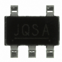
S-8354A33MC-JQST2G Seiko Instruments, S-8354A33MC-JQST2G Datasheet - Page 8

S-8354A33MC-JQST2G
Manufacturer Part Number
S-8354A33MC-JQST2G
Description
IC SWITCHING REG 3.3V SOT-23-5
Manufacturer
Seiko Instruments
Type
Step-Up (Boost)r
Datasheet
1.S-8354A33MC-JQST2G.pdf
(49 pages)
Specifications of S-8354A33MC-JQST2G
Internal Switch(s)
Yes
Synchronous Rectifier
No
Number Of Outputs
1
Voltage - Output
3.3V
Frequency - Switching
50kHz
Voltage - Input
0.9 ~ 10 V
Operating Temperature
-40°C ~ 85°C
Mounting Type
Surface Mount
Package / Case
SOT-23-5, SC-74A, SOT-25
Power - Output
250mW
Output Voltage
3.3 V
Input Voltage
10 V
Duty Cycle (max)
90 %
Switching Frequency
50 KHz
Mounting Style
SMD/SMT
Primary Input Voltage
3.8V
No. Of Outputs
1
Output Current
231mA
No. Of Pins
5
Operating Temperature Range
-40°C To +85°C
Operating Temperature Min
85°C
Rohs Compliant
Yes
Lead Free Status / RoHS Status
Lead free / RoHS Compliant
Current - Output
-
Lead Free Status / Rohs Status
Lead free / RoHS Compliant
Other names
728-1035-2
Available stocks
Company
Part Number
Manufacturer
Quantity
Price
Part Number:
S-8354A33MC-JQST2G
Manufacturer:
SEIKO/精工
Quantity:
20 000
8
STEP-UP, PWM CONTROL or PWM / PFM SWITCHABLE BUILT-IN TRANSISTOR SWITCHING REGULATOR
S-8353/8354 Series
Pin Configurations
1
5
1
2
SOT-23-3
SOT-89-3
SOT-23-5
Top view
Top view
Figure 4
Top view
Figure 5
Figure 6
2
2
1
4
3
3
3
*1. The NC pin indicates electrically open.
*1. The NC pin indicates electrically open.
Pin No.
Pin No.
Pin No.
Pin No.
Seiko Instruments Inc.
1
2
3
1
2
3
4
5
1
2
3
4
5
1
2
3
(Without shutdown function, V
(Without shutdown function, V
(With shutdown function, V
(Without shutdown function, V
ON
Symbol
Symbol
Symbol
Symbol
VOUT
CONT
VOUT
CONT
VOUT
CONT
VOUT
CONT
NC
VDD
NC
VSS
VSS
VSS
VSS
/
OFF
*1
*1
Table 9 A, C and H Types
Table 10 A and H Types
Table 12 A and H Types
Table 11 D and J Types
Output voltage pin and IC power supply pin
GND pin
External inductor connection pin
Shutdown pin
Output voltage pin and IC power supply pin
No connection
GND pin
External inductor connection pin
Output voltage pin
IC power supply pin
No connection
GND pin
External inductor connection pin
GND pin
Output voltage pin and IC power supply pin
External inductor connection pin
“H”: Normal operation (Step-up operating)
“L”: Step-up stopped (Entire circuit stopped)
DD
DD
DD
/ V
DD
/ V
/ V
OUT
Description
Description
Description
Description
/ V
OUT
OUT
non-separate type)
OUT
non-separate type)
non-separate type)
separate type)
Rev.3.0
_00


