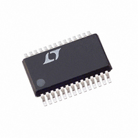
LTC3729EG#PBF Linear Technology, LTC3729EG#PBF Datasheet - Page 25

LTC3729EG#PBF
Manufacturer Part Number
LTC3729EG#PBF
Description
IC SW REG SYNC STEP-DOWN 28-SSOP
Manufacturer
Linear Technology
Series
PolyPhase®r
Type
Step-Down (Buck)r
Datasheet
1.LTC3729EGPBF.pdf
(30 pages)
Specifications of LTC3729EG#PBF
Internal Switch(s)
No
Synchronous Rectifier
Yes
Number Of Outputs
1
Voltage - Output
0.8 ~ 5 V
Current - Output
5A
Frequency - Switching
1.1MHz
Voltage - Input
4 ~ 36 V
Operating Temperature
-40°C ~ 85°C
Mounting Type
Surface Mount
Package / Case
28-SSOP
Primary Input Voltage
36V
No. Of Outputs
1
Output Current
5A
No. Of Pins
28
Operating Temperature Range
-40°C To +85°C
Msl
MSL 1 - Unlimited
Supply Voltage Range
4V To 36V
Rohs Compliant
Yes
Lead Free Status / RoHS Status
Lead free / RoHS Compliant
Power - Output
-
Available stocks
Company
Part Number
Manufacturer
Quantity
Price
APPLICATIONS INFORMATION
Simplified Visual Explanation of How a 2-Phase
Controller Reduces Both Input and Output RMS Ripple
Current
A multiphase power supply significantly reduces the amount
of ripple current in both the input and output capacitors.
The RMS input ripple current is divided by, and the effective
ripple frequency is multiplied up by the number of phases
used (assuming that the input voltage is greater than the
number of phases used times the output voltage). The output
ripple amplitude is also reduced by, and the effective ripple
frequency is increased by the number of phases used. Figure
10 graphically illustrates the principle.
The worst‑case RMS ripple current for a single stage design
peaks at twice the value of the output voltage . The worst‑
case RMS ripple current for a two stage design results in
peaks at 1/4 and 3/4 of input voltage. When the RMS cur‑
rent is calculated, higher effective duty factor results and
the peak current levels are divided as long as the currents
in each stage are balanced. Refer to Application Note 19 for
a detailed description of how to calculate RMS current for
the single stage switching regulator. Figures 3 and 4 help to
Figure 10. Single and PolyPhase Current Waveforms
SW1 V
SW2 V
SW V
I
I
COUT
COUT
I
I
CIN
CIN
I
I
L1
L2
SINGLE PHASE
DUAL PHASE
RIPPLE
3729
F10
illustrate how the input and output currents are reduced by
using an additional phase. The input current peaks drop in
half and the frequency is doubled for a 2‑phase converter.
The input capacity requirement is reduced theoretically by a
factor of four! A ceramic input capacitor with its unbeatably
low ESR characteristic can be used.
Figure 4 illustrates the RMS input current drawn from the
input capacitance versus the duty cycle as determined
by the ratio of input and output voltage. The peak input
RMS current level of the single phase system is reduced
by 50% in a 2‑phase solution due to the current splitting
between the two stages.
An interesting result of the multi‑phase solution is that the
V
capacitor, V
zero input current ripple in the 2‑phase design.
The output ripple current is reduced significantly when
compared to the single phase solution using the same
inductance value because the V
term from the stage(s) that has its bottom MOSFET on
subtracts current from the (V
resulting from the stage which has its top MOSFET on.
The output ripple current is:
where D is duty factor.
The input and output ripple frequency is increased by
the number of stages used, reducing the output capacity
requirements. When V
as illustrated in Figures 3 and 4, very low input and output
ripple currents result.
Again, the interesting result of 2‑phase operation results
in no output ripple at V
phases by phase locking additional controllers always
results in no net input or output ripple at V
equal to the number of stages implemented. Designing a
system with a multiple of stages close to the V
will significantly reduce the ripple voltage at the input and
outputs and thereby improve efficiency, physical size, and
heat generation of the overall switching power supply.
IN
I
RIPPLE
which produces worst‑case ripple current for the input
=
OUT
2V
= V
fL
OUT
IN
/2, in the single phase design produces
1− 2D 1−D
IN
1− 2D + 1
OUT
is approximately equal to NV
= V
(
IN
IN
‑ V
OUT
/2. The addition of more
)
OUT
/L discharge current
)/L charging current
LTC3729
OUT
OUT
/V
/V
IN
25
IN
ratios
ratio
3729fb
OUT


