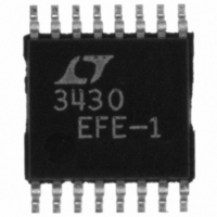
LT3430EFE-1#PBF Linear Technology, LT3430EFE-1#PBF Datasheet - Page 7

LT3430EFE-1#PBF
Manufacturer Part Number
LT3430EFE-1#PBF
Description
IC REG 3A HV SW 16-TSSOP
Manufacturer
Linear Technology
Type
Step-Down (Buck)r
Datasheet
1.LT3430EFE-1PBF.pdf
(28 pages)
Specifications of LT3430EFE-1#PBF
Internal Switch(s)
Yes
Synchronous Rectifier
No
Number Of Outputs
1
Voltage - Output
1.2 ~ 54 V
Current - Output
3A
Frequency - Switching
100kHz
Voltage - Input
5.5 ~ 60 V
Operating Temperature
-40°C ~ 125°C
Mounting Type
Surface Mount
Package / Case
16-TSSOP Exposed Pad, 16-eTSSOP, 16-HTSSOP
Lead Free Status / RoHS Status
Lead free / RoHS Compliant
Power - Output
-
Available stocks
Company
Part Number
Manufacturer
Quantity
Price
BLOCK DIAGRAM
The LT3430/LT3430-1 are constant frequency, current
mode buck converters. This means that there is an in-
ternal clock and two feedback loops that control the duty
cycle of the power switch. In addition to the normal error
amplifi er, there is a current sense amplifi er that monitors
switch current on a cycle-by-cycle basis. A switch cycle
starts with an oscillator pulse which sets the R
to turn the switch on. When switch current reaches a level
set by the inverting input of the comparator, the fl ip-fl op
is reset and the switch turns off. Output voltage control is
obtained by using the output of the error amplifi er to set
the switch current trip point. This technique means that the
error amplifi er commands current to be delivered to the
output rather than voltage. A voltage fed system will have
low phase shift up to the resonant frequency of the inductor
and output capacitor, then an abrupt 180° shift will occur.
The current fed system will have 90° phase shift at a much
lower frequency, but will not have the additional 90° shift
until well beyond the LC resonant frequency. This makes
SHDN
SYNC
BIAS
V
IN
COMPARATOR
3, 4
10
14
15
SHUTDOWN
REGULATOR
+
2.9V BIAS
2.38V
0.4V
–
+
–
COMPARATOR
LOCKOUT
5.5µA
INTERNAL
V
CC
ANTISLOPE COMP
100kHz: LT3430-1
200kHz: LT3430
SLOPE COMP
OSCILLATOR
Figure 1. LT3430/LT3430-1 Block Diagram
S
fl ip-fl op
V
CLAMP
C(MAX)
Σ
Q3
+
×1
11
V
R
it much easier to frequency compensate the feedback loop
and also gives much quicker transient response.
Most of the circuitry of the LT3430/LT3430-1 operates
from an internal 2.9V bias line. The bias regulator normally
draws power from the regulator input pin, but if the BIAS
pin is connected to an external voltage equal to or higher
than 3V, bias power will be drawn from the external source
(typically the regulated output voltage). This will improve
effi ciency if the BIAS pin voltage is lower than regulator
input voltage.
High switch effi ciency is attained by using the BOOST pin
to provide a voltage to the switch driver which is higher
than the input voltage, allowing switch to be saturated.
This boosted voltage is generated with an external ca-
pacitor and diode. Two comparators are connected to the
shutdown pin. One has a 2.38V threshold for undervoltage
lockout and the second has a 0.4V threshold for complete
shutdown.
C
LIMIT
FOLDBACK
CURRENT
–
CLAMP
LIMIT
CURRENT
COMPARATOR
Q2
S
R
FLIP-FLOP
g
R
m
S
FREQUENCY
= 2000µMho
FOLDBACK
AMPLIFIER
ERROR
BOOST
LT3430/LT3430-1
CIRCUITRY
6
DRIVER
–
+
1.22V
3430 F01
2, 5
12
Q1
POWER
SWITCH
R
SENSE
SW
FB
GND
1, 8, 9, 16, 17
34301fa
7


