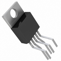
LT1171CT#PBF Linear Technology, LT1171CT#PBF Datasheet - Page 11

LT1171CT#PBF
Manufacturer Part Number
LT1171CT#PBF
Description
IC SW-REG HI-EFF 2.5A TO220-5
Manufacturer
Linear Technology
Type
Step-Down (Buck), Step-Up (Boost), Inverting, Cuk, Flyback, Forward Converterr
Datasheet
1.LT1172CN8PBF.pdf
(24 pages)
Specifications of LT1171CT#PBF
Internal Switch(s)
Yes
Synchronous Rectifier
No
Number Of Outputs
1
Voltage - Output
1.25 ~ 40 V
Current - Output
2.5A
Frequency - Switching
100kHz
Voltage - Input
3 ~ 40 V
Operating Temperature
0°C ~ 100°C
Mounting Type
Through Hole
Package / Case
TO-220-5 (Bent and Staggered Leads)
Power - Output
100W
Primary Input Voltage
60V
No. Of Outputs
1
Output Voltage
65V
Output Current
5.5A
No. Of Pins
5
Operating Temperature Range
0°C To +100°C
Msl
MSL 1 - Unlimited
Supply Voltage Range
3V To 40V
Rohs Compliant
Yes
Dc To Dc Converter Type
Non-Inverting/Inverting/Step Up/Step Down
Pin Count
5 +Tab
Input Voltage
40V
Switching Freq
85 TO 115KHz
Package Type
TO-220
Output Power (max)
100W
Output Type
Adjustable
Switching Regulator
Yes
Line Regulation
0.03%/V
Mounting
Through Hole
Input Voltage (min)
3V
Operating Temperature Classification
Commercial
Lead Free Status / RoHS Status
Lead free / RoHS Compliant
Available stocks
Company
Part Number
Manufacturer
Quantity
Price
OPERATION
TYPICAL APPLICATIONS
With t
voltage shift is ≈ 3.8mV. This is not particularly bother-
some, but note that high offsets could result if R3 were
reduced to a much lower value. Also, the synchronizing
100μF
C4*
20V TO 30V
+
S
GND
= 0.2μs, f
V
V
IN
IN
LT1170
Synchronizing with Bipolar Transistor
GND
*REQUIRED IF INPUT LEADS ≥ 2"
LT1170
S
V
V
C
= 150kHz, V
IN
R3
C1
V
C
2N2369
V
R3
1.5k
SW
FB
C2
0.15μF
C
= 1.5V, and R3 = 2k, offset
D2
MUR110
D3
25V
1W
R2
2.2k
39pF
C2
N* = 1/3
R1
1
3k
N*
FROM 5V
1170/1/2 OP01
LOGIC
D1
Flyback Converter
+
100μF
5μH
L2
C4
C1
2000μF
OPTIONAL
FILTER
transistor must sink higher currents with low values of
R3, so larger drives may have to be used. The transistor
must be capable of pulling the V
ground to ensure synchronizing.
R2
1.24k
R1
3.74k
V
5V
6A
OUT
GND
V
IN
LT1170
V
0V
0V
IN
0
0
0
0
LT1170/LT1171/LT1172
Synchronizing with MOS Transistor
V
V
C
a
I
PRI
SNUB
c
R3
I
C1
t =
(I
b
d
PRI
V
* SILICONIX OR EQUIVALENT
VN2222*
SNUB
V
)(L
I
I
OUT
PRI
PRI
L
)
CLAMP TURN-ON
+ V
I
N • V
PRI
f
/N
SPIKE
IN
PRIMARY FLYBACK VOLTAGE =
LT1170 SWITCH VOLTAGE
AREA “a” = AREA “b” TO MAINTAIN
ZERO DC VOLTS ACROSS PRIMARY
SECONDARY VOLTAGE
AREA “c” = AREA “d” TO MAINTAIN
ZERO DC VOLTS ACROSS SECONDARY
PRIMARY CURRENT
SECONDARY CURRENT
LT1170 SWITCH CURRENT
SNUBBER DIODE CURRENT
R2
2.2k
C
1N4158
pin to within 200mV of
D1
D2
1N4158
100pF
C2
1170/1/2 TA03
FROM 5V
1170/1/2 OP02
LOGIC
11
V
OUT
117012fg
N
+ Vf


