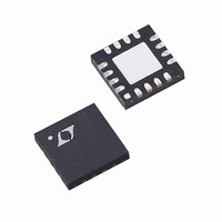
LT3689EUD#PBF Linear Technology, LT3689EUD#PBF Datasheet - Page 14

LT3689EUD#PBF
Manufacturer Part Number
LT3689EUD#PBF
Description
IC SWIT REG BUCK 700MA ADJ 16QFN
Manufacturer
Linear Technology
Type
Step-Down (Buck)r
Datasheet
1.LT3689EUDPBF.pdf
(32 pages)
Specifications of LT3689EUD#PBF
Internal Switch(s)
Yes
Synchronous Rectifier
No
Number Of Outputs
1
Voltage - Output
0.8 ~ 34.2 V
Current - Output
700mA
Frequency - Switching
350kHz ~ 2.2MHz
Voltage - Input
3.6 ~ 36 V
Operating Temperature
-40°C ~ 125°C
Mounting Type
Surface Mount
Package / Case
16-WQFN Exposed Pad
Lead Free Status / RoHS Status
Lead free / RoHS Compliant
Power - Output
-
Available stocks
Company
Part Number
Manufacturer
Quantity
Price
LT3689/LT3689-5
Maximum Operating Voltage
The maximum input voltage for LT3689 applications
depends on switching frequency, the absolute maximum
ratings of the V
duty cycle (DC
voltages up to 36V, and safely withstand input transient
voltages up to 60V. Note that while V
the LT3689 will stop switching, allowing the output to fall
out of regulation.
where t
is equal to 150ns) and f
Running at a lower switching frequency allows a lower
minimum duty cycle. The maximum input voltage before
pulse-skipping occurs depends on the output voltage and
the minimum duty cycle:
Example: f
The LT3689 will regulate the output current at input volt-
ages greater than V
APPLICATIONS INFORMATION
14
DC
V
V
IN(PS)
IN(PS)
MIN
ON(MIN)
50mV/DIV
0.5A/DIV
= t
DC
=
SW
=
V
Figure 1. Operation Below V
V
(AC)
ON(MIN)
OUT
MIN
OUT
3.3V + 0.4V
V
I
= 790kHz, V
L
OUT
DC
MIN
is equal to 130ns (for T
0.103
= 1.8V and f
IN
= 130ns • 790kHz = 0.103
MIN
). The LT3689 can operate from input
+ V
and BST pins, and by the minimum
• f
IN(PS)
D
SW
– V
SW
OUT
– 0.4V + 0.4V = 36V
. For example, an application
SW
5µs/DIV
D
is the switching frequency.
+ V
= 1.5MHz
= 3.3V,
SW
IN(PS)
IN
J
> 125°C t
. V
> 38V (typical),
3689 F01
IN
= 10V,
ON(MIN)
with an output voltage of 1.8V and switching frequency
of 1.5MHz has a V
Figure 2 shows operation at 24V. Output ripple and peak
inductor current have significantly increased. A saturating
inductor may further reduce performance. For input volt-
ages over 30V, there are restrictions on the inductor size
and saturation rating. See the Inductor Selection section
for more details. In pulse-skipping mode, the LT3689 skips
switching pulses to maintain output regulation. Above 38V
(typical) switching will stop. Transients of up to 60V are
acceptable, regardless of switching frequency.
Minimum Operating Voltage Range
The minimum input voltage is determined either by the
LT3689’s minimum operating voltage of ~3.4V or by its
maximum duty cycle. The duty cycle is the fraction of
time that the internal switch is on and is determined by
the input and output voltages:
Unlike many fixed frequency regulators, the LT3689 can
extend its duty cycle by remaining on for multiple cycles.
The LT3689 will not switch off at the end of each clock cycle
if there is sufficient voltage across the boost capacitor (C3
in the Block Diagram). Eventually, the voltage on the boost
capacitor falls and requires refreshing. Circuitry detects
DC =
50mV/DIV
V
0.5A/DIV
IN
Figure 2. Operation Above V
V
and Peak Inductor Current Increase
V
V
OUT
(AC)
OUT
OUT
– V
I
L
= 1.8V and f
SW
+ V
+ V
IN(PS)
D
D
of 11.3V, as shown in
SW
5µs/DIV
= 1.5MHz. Output Ripple
IN(PS)
. V
3689 F02
IN
= 24V,
Figure
3689fd
1.


