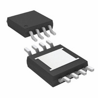
LT3663IMS8E#PBF Linear Technology, LT3663IMS8E#PBF Datasheet - Page 10

LT3663IMS8E#PBF
Manufacturer Part Number
LT3663IMS8E#PBF
Description
IC BUCK 1.2A ADJ 8MSOP
Manufacturer
Linear Technology
Type
Step-Down (Buck)r
Datasheet
1.LT3663EDCBTRMPBF.pdf
(16 pages)
Specifications of LT3663IMS8E#PBF
Internal Switch(s)
Yes
Synchronous Rectifier
No
Number Of Outputs
1
Voltage - Output
1.2 ~ 33.12 V
Current - Output
1.2A
Frequency - Switching
1.5MHz
Voltage - Input
7.5 ~ 36 V
Operating Temperature
-40°C ~ 125°C
Mounting Type
Surface Mount
Package / Case
8-MSOP Exposed Pad, 8-HMSOP, 8-eMSOP
Lead Free Status / RoHS Status
Lead free / RoHS Compliant
Power - Output
-
Available stocks
Company
Part Number
Manufacturer
Quantity
Price
LT3663
BOOST and BIAS Pin Considerations
Capacitor C3 and the internal boost diode (see the Block
Diagram) are used to generate a boost voltage that is higher
than the input voltage. In most cases a 0.1μF capacitor
works well. Figure 4 shows three ways to arrange the boost
circuit. The BOOST pin must be more than 2.3V above the
SW pin for best effi ciency. For outputs of 3V and above, the
standard circuit (Figure 4a) is best. For outputs between
2.8V and 3V, use a 1μF boost capacitor. A 2.5V output
presents a special case because it is marginally adequate
to support the boosted drive stage while using the internal
APPLICATIONS INFORMATION
10
V
IN
(4a) For V
V
IN
LT3663
Figure 4. Three Circuits to Generate BOOST Pin Voltage
OUT
BOOST
I
SENSE
V
> 2.8V
OUT
SW
(4c) For V
V
IN
C3
OUT
V
V
OUT
IN
< 2.5V; V
LT3663
D3
BOOST
boost diode. For reliable BOOST pin operation with 2.5V
outputs use a good external Schottky diode (such as the
ON Semi, MBR0540) and a 1μF boost capacitor (see Figure
4b). For lower output voltages connect an external Schottky
diode to the input (Figure 4c), or to another supply greater
than 2.8V. Using V
to 25V. The circuit in Figure 4a is more effi cient because
the BOOST pin current comes from a lower voltage source.
Take care to ensure that the maximum voltage ratings of
the BOOST pin is not exceeded.
I
SENSE
V
OUT
SW
IN(MAX)
V
IN
(4b) For 2.5V < V
= 25V
3663 F04
C3
V
IN
V
LT3663
OUT
IN
reduces the maximum input voltage
BOOST
I
SENSE
OUT
V
OUT
SW
< 2.8V
C3
D3
V
OUT
3663fb


