TC962COE Microchip Technology, TC962COE Datasheet - Page 3
TC962COE
Manufacturer Part Number
TC962COE
Description
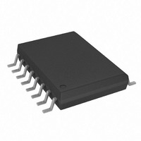
IC CHARGE PUMP DC/DC CONV 16SOIC
Manufacturer
Microchip Technology
Type
Switched Capacitor (Charge Pump), Invertingr
Datasheet
1.TC962COE.pdf
(12 pages)
Specifications of TC962COE
Package / Case
16-SOIC (0.300", 7.5mm Width)
Internal Switch(s)
Yes
Synchronous Rectifier
No
Number Of Outputs
1
Voltage - Output
-3 ~ -18 V
Current - Output
80mA
Frequency - Switching
12kHz ~ 24kHz
Voltage - Input
3 ~ 18 V
Operating Temperature
0°C ~ 70°C
Mounting Type
Surface Mount
Power - Output
760mW
Minimum Operating Temperature
0 C
Mounting Style
SMD/SMT
Function
Inverting
Output Voltage
- 18 V to - 3 V
Output Current
80 mA (Max)
Maximum Operating Temperature
+ 70 C
Lead Free Status / RoHS Status
Lead free / RoHS Compliant
Lead Free Status / RoHS Status
Lead free / RoHS Compliant, Lead free / RoHS Compliant
Available stocks
Company
Part Number
Manufacturer
Quantity
Price
Company:

Part Number:
TC962COE713
Manufacturer:
MICROCHIP
Quantity:
12 000


1.0
Absolute Maximum Ratings*
Supply Voltage (V
Input Voltage Any Pin
Current Into Any Pin........................................... 10 mA
ESD Protection ................................................ ±2000V
Output Short Circuit ........... Continuous (at 5.5V Input)
Package Power Dissipation (T
Package Thermal Resistance
Operating Temperature Range
Storage Temperature Range ............. -65°C to +150°C
TC962 ELECTRICAL SPECIFICATIONS
© 2006 Microchip Technology Inc.
Electrical Characteristics: V
V
I
R
F
P
V
V
Z
Note
S
DD
OSC
EFF
DEF
Z
ZT
O
Symbol
SOIC ....................................................... 760 mW
PDIP........................................................ 730 mW
CERDIP .................................................. 800 mW
CERDIP, Rθ
PDIP, Rθ
CPA, COE ....................................... 0°C to +70°C
IJA ................................................ -25°C to +85°C
EPA .............................................. -40°C to +85°C
MJA ............................................ -55°C to +125°C
......................... (V
1:
ELECTRICAL
CHARACTERISTICS
Connecting any input terminal to voltages greater than V
inputs from sources operating from external supplies be applied prior to “power-up” of the TC962.
J-A
Supply Voltage
Supply Current
V
V
Output Source
Resistance
Oscillator Frequency
Power Efficiency
Voltage Efficiency
Zener Voltage
Zener Impedance
DD
DD
............................................ 140°C/W
J-A
DD
= 15V
= 5V
......................................... 90°C/W
to GND) ..............................+18V
DD
Parameter
+0.3) to (V
DD
A
= 15V, T
≤ 70°C)
A
SS
= 25°C (See Figure ) unless otherwise noted.
-0.3) (Note 1)
Min
6.0
93
99
96
—
—
—
—
—
—
—
—
—
—
—
—
—
—
—
3
+
99.9
or less than GND may cause destructive latch-up. It is recommended that no
Typ
510
560
650
190
210
210
6.2
32
35
12
24
97
12
—
—
—
—
—
—
*Stresses
Maximum Ratings” may cause permanent damage to
the device. These are stress ratings only and functional
operation of the device at these or any other conditions
above those indicated in the operation sections of the
specifications is not implied. Exposure to Absolute
Maximum Rating conditions for extended periods may
affect device reliability.
Max
700
6.4
18
—
—
—
—
—
—
37
40
50
—
—
—
—
—
—
—
—
Units
above
kHz
μA
%
%
Ω
Ω
V
V
R
T
0 ≤ T
-55°C ≤ T
T
0 ≤ T
-55°C ≤ T
I
I
I
Pin 6 Open
Pin 6 GND
R
R
Over temperature range
I
I
L
L
L
Z
L
those
A
A
L
L
L
= 20 mA, V
= 80 mA, V
= 3 mA, V
= 2.5 mA to 7.5 mA
= 5 mA
= +25°C
= +25°C
= ∞
= 2 kΩ
= ∞
A
A
≤ +70°C
≤ +70°C
A
A
listed
Test Conditions
≤ +125°C
≤ +125°C
DD
DD
DD
= 5V
= 15V
= 15V
under
DS21484C-page 3
TC962
“Absolute
Related parts for TC962COE
Image
Part Number
Description
Manufacturer
Datasheet
Request
R

Part Number:
Description:
Manufacturer:
Microchip Technology Inc.
Datasheet:
Part Number:
Description:
Manufacturer:
Microchip Technology Inc.
Datasheet:
Part Number:
Description:
Manufacturer:
Microchip Technology Inc.
Datasheet:
Part Number:
Description:
Manufacturer:
Microchip Technology Inc.
Datasheet:
Part Number:
Description:
Manufacturer:
Microchip Technology Inc.
Datasheet:
Part Number:
Description:
Manufacturer:
Microchip Technology Inc.
Datasheet:
Part Number:
Description:
Manufacturer:
Microchip Technology Inc.
Datasheet:
Part Number:
Description:
Manufacturer:
Microchip Technology Inc.
Datasheet: