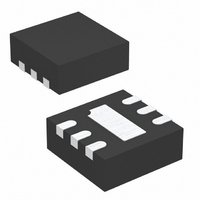
LTC3240EDC-3.3#TRMPBF Linear Technology, LTC3240EDC-3.3#TRMPBF Datasheet - Page 5

LTC3240EDC-3.3#TRMPBF
Manufacturer Part Number
LTC3240EDC-3.3#TRMPBF
Description
IC DC/DC CONV 3.3V 6-DFN
Manufacturer
Linear Technology
Type
Step-Down (Buck), Step-Up (Boost), Switched Capacitor (Charge Pump)r
Datasheet
1.LTC3240EDC-3.3TRMPBF.pdf
(12 pages)
Specifications of LTC3240EDC-3.3#TRMPBF
Internal Switch(s)
Yes
Synchronous Rectifier
No
Number Of Outputs
1
Voltage - Output
3.3V
Current - Output
150mA
Frequency - Switching
1.2MHz
Voltage - Input
1.8 ~ 5.5 V
Operating Temperature
-40°C ~ 85°C
Mounting Type
Surface Mount
Package / Case
6-DFN
Operating Supply Voltage (min)
1.8V
Operating Supply Voltage (max)
5.5V
Operating Temp Range
-40C to 85C
Operating Temperature Classification
Industrial
Package Type
DFN
Pin Count
6
Mounting
Surface Mount
Lead Free Status / RoHS Status
Lead free / RoHS Compliant
Power - Output
-
Lead Free Status / Rohs Status
Compliant
Other names
LTC3240EDC-3.3#TRMPBF
LTC3240EDC-3.3#TRMPBFTR
LTC3240EDC-3.3#TRMPBFTR
Available stocks
Company
Part Number
Manufacturer
Quantity
Price
Part Number:
LTC3240EDC-3.3#TRMPBFLTC3240EDC-3.3#PBF
Manufacturer:
LINEAR/凌特
Quantity:
20 000
PI FU CTIO S
AC COUPLED
GND (Pin 1): Ground. This pin should be tied to a ground
plane for best performance.
V
with a 1μF or greater, low ESR ceramic capacitor.
V
bypassed with a 4.7μF or greater, low ESR ceramic capaci-
tor as close to the pin as possible for best performance.
C
TYPICAL PERFOR A CE CHARACTERISTICS
unless otherwise noted)
I
IN
OUT
+
LOAD
20mV/DIV
U
(Pin 4): Flying Capacitor Positive Terminal.
(Pin 2): Input Supply Voltage. V
60mA
10mA
V
(Pin 3): Regulated Output Voltage. V
OUT
V
I
Load Transient Response
(LTC3240-3.3)
LOAD
IN
U
= 3.7V
= 10mA TO 60mA
LDO MODE
10µs/DIV
U
W
U
IN
3240 G15
should be bypassed
AC COUPLED
20mV/DIV
OUT
V
OUT
should be
V
I
Output Noise/Ripple
(LTC3240-2.5)
LOAD
IN
= 2.4V
= 100mA
500ns/DIV
C
⎯ S ⎯ H ⎯ D ⎯ N (Pin 6): Active Low Shutdown Input. A low on ⎯ S ⎯ H ⎯ D ⎯ N
disables the LTC3240-3.3/LTC3240-2.5. This pin is a high
impedance CMOS input pin which must be driven with valid
logic levels. This pin must not be allowed to fl oat.
Exposed Pad (Pin 7): Ground. The exposed pad must be
soldered to PCB ground to provide electrical contact and
optimum thermal performance.
–
(Pin 5): Flying Capacitor Negative Terminal.
LTC3240-3.3/LTC3240-2.5
(T
A
3240 G16
= 25°C, C
AC COUPLED
I
LOAD
20mV/DIV
50mA
10mA
V
FLY
OUT
= C
V
I
Load Transient Response
(LTC3240-2.5)
LOAD
IN
OPERATION
IN
Burst Mode
= 2.4V
= 10mA TO 50mA
= 1µF, C
OUT
CONST FREQUENCY
10µs/DIV
= 4.7µF
MODE
3240fb
5
3240 G17


