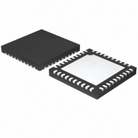
ISL6566CRZ-T Intersil, ISL6566CRZ-T Datasheet - Page 6

ISL6566CRZ-T
Manufacturer Part Number
ISL6566CRZ-T
Description
IC CTLR PWM BUCK 3PHASE 40-QFN
Manufacturer
Intersil
Datasheet
1.ISL6566CRZ-TR5184.pdf
(29 pages)
Specifications of ISL6566CRZ-T
Applications
Controller, Intel VRM9, VRM10, and AMD Hammer Applications
Voltage - Input
3 ~ 12 V
Number Of Outputs
1
Voltage - Output
0.84 ~ 1.6 V
Operating Temperature
0°C ~ 70°C
Mounting Type
Surface Mount
Package / Case
40-VFQFN, 40-VFQFPN
Lead Free Status / RoHS Status
Lead free / RoHS Compliant
Other names
ISL6566CRZ-TCT
Available stocks
Company
Part Number
Manufacturer
Quantity
Price
Company:
Part Number:
ISL6566CRZ-T
Manufacturer:
INTERSIL
Quantity:
3 340
Absolute Maximum Ratings
Supply Voltage, VCC . . . . . . . . . . . . . . . . . . . . . . . . . . . -0.3V to +6V
Supply Voltage, PVCC . . . . . . . . . . . . . . . . . . . . . . . . . -0.3V to +15V
Absolute Boot Voltage, V
Phase Voltage, V
Upper Gate Voltage, V
Lower Gate Voltage, V
Input, Output, or I/O Voltage . . . . . . . . . GND - 0.3V to VCC + 0.3V
ESD Classification . . . . . . . . . . . . . . . . . . . . . . . Class I JEDEC STD
Recommended Operating Conditions
VCC Supply Voltage . . . . . . . . . . . . . . . . . . . . . . . . . . . . . +5V ±5%
PVCC Supply Voltage . . . . . . . . . . . . . . . . . . . . . . . +5V to 12V ±5%
Ambient Temperature (ISL6566CR, ISL6566CRZ) . . . . 0°C to 70°C
Ambient Temperature (ISL6566IR, ISL6566IRZ) . . . . .-40°C to 85°C
CAUTION: Stress above those listed in “Absolute Maximum Ratings” may cause permanent damage to the device. This is a stress only rating and operation of the
device at these or any other conditions above those indicated in the operational section of this specification is not implied.
NOTES:
Electrical Specifications
BIAS SUPPLY AND INTERNAL OSCILLATOR
Input Bias Supply Current
Gate Drive Bias Current
VCC POR (Power-On Reset) Threshold
PVCC POR (Power-On Reset) Threshold
Oscillator Ramp Amplitude (Note 3)
Maximum Duty Cycle (Note 3)
Oscillator Frequency, F
CONTROL THRESHOLDS
ENLL Rising Threshold
ENLL Hysteresis
COMP Shutdown Threshold
REFERENCE AND DAC
System Accuracy (VID = 1.0V - 1.850V)
System Accuracy (VID = 0.8V - 1.0V)
DAC Input Low Voltage (VR9, VR10)
DAC Input High Voltage (VR9, VR10)
DAC Input Low Voltage (AMD)
DAC Input High Voltage (AMD)
OFS Sink Current Accuracy (Negative Offset)
OFS Source Current Accuracy (Positive Offset)
1. θ
2. For θ
Tech Brief TB379.
GND - 8V (<400ns, 20µJ) to 24V (<200ns, V
JA
V
is measured in free air with the component mounted on a high effective thermal conductivity test board with “direct attach” features. See
PHASE
JC
, the “case temp” location is the center of the exposed metal pad on the package underside.
GND - 5V (<100ns Pulse Width, 2µJ) to PVCC+ 0.3V
- 3.5V (<100ns Pulse Width, 2µJ) to V
PHASE
PARAMETER
UGATE
LGATE
SW
BOOT
. . . . . . . . GND - 0.3V to 15V (PVCC = 12)
. . . . . . . . GND - 0.3V to PVCC + 0.3V
. . . . V
. . . . . . . . GND - 0.3V to GND + 36V
6
Recommended Operating Conditions, Unless Otherwise Specified.
PHASE
- 0.3V to V
BOOT-PHASE
I
I
VCC Rising
VCC Falling
PVCC Rising
PVCC Falling
V
R
COMP Falling
R
R
VCC
PVCC
BOOT
BOOT
PP
T
OFS
OFS
= 100kΩ (
; ENLL = high
; ENLL = high
= 30kΩ from OFS to VCC
= 10kΩ from OFS to GND
+ 0.3V
+ 0.3V
= 12V)
ISL6566
ISL6566
±
0.1%)
TEST CONDITIONS
Thermal Information
Thermal Resistance
Maximum Junction Temperature . . . . . . . . . . . . . . . . . . . . . . . 150°C
Maximum Storage Temperature Range . . . . . . . . . . . -65°C to 150°C
Maximum Lead Temperature (Soldering 10s) . . . . . . . . . . . . . 300°C
QFN Package (Notes 1, 2) . . . . . . . . . .
4.25
3.75
4.25
3.60
47.5
47.5
MIN
225
-0.5
-0.8
0.2
0.8
1.0
-
-
-
-
-
-
-
-
TYP
4.38
3.88
4.38
3.88
1.50
66.6
0.66
50.0
50.0
250
100
0.8
0.3
15
θ
-
-
-
-
-
-
JA
(°C/W)
32
MAX
4.50
4.00
4.50
4.00
52.5
52.5
275
0.4
0.5
0.8
0.4
0.6
20
-
-
-
-
-
-
-
θ
March 9, 2006
JC
FN9178.4
3.5
UNITS
(°C/W)
kHz
mA
mA
mV
µA
µA
%
%
%
V
V
V
V
V
V
V
V
V
V
V


