ISL6563CR-T Intersil, ISL6563CR-T Datasheet - Page 9
ISL6563CR-T
Manufacturer Part Number
ISL6563CR-T
Description
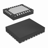
IC CTRLR PWM MULTIPHASE 24-QFN
Manufacturer
Intersil
Datasheet
1.ISL6563IR.pdf
(19 pages)
Specifications of ISL6563CR-T
Applications
Controller, Intel VRM9, VRM10, and AMD Hammer Applications
Voltage - Input
5 ~ 12 V
Number Of Outputs
1
Voltage - Output
0.8 ~ 1.85 V
Operating Temperature
0°C ~ 70°C
Mounting Type
Surface Mount
Package / Case
24-VQFN Exposed Pad, 24-HVQFN, 24-SQFN, 24-DHVQFN
Lead Free Status / RoHS Status
Contains lead / RoHS non-compliant
Available stocks
Company
Part Number
Manufacturer
Quantity
Price
Company:

Part Number:
ISL6563CR-T
Manufacturer:
ICS
Quantity:
13 000


PWM OPERATION
One switching cycle for the ISL6563 is defined as the time
between consecutive PWM pulse terminations (turn-off of
the upper MOSFET on a channel). Each cycle begins when
a switching clock signal commands the upper MOSFET to
go off. The other channel’s upper MOSFET conduction is
terminated 1/2 of a cycle later.
Once a channel’s upper MOSFET is turned off, the lower
MOSFET remains on for a minimum of 1/3 cycle. This forced
off time is required to assure an accurate current sample.
Following the 1/3-cycle forced off time, the controller enables
the upper MOSFET output. Once enabled, the upper
MOSFET output transitions high when the sawtooth signal
crosses the adjusted error-amplifier output signal, as
illustrated in the ISL6563’s block diagram. Just prior to the
upper drive turning the MOSFET on, the lower MOSFET
drive turns the freewheeling element off. The upper
MOSFET is kept on until the clock signals the beginning of
the next switching cycle and the PWM pulse is terminated.
CURRENT SENSING
ISL6563 senses current by sampling the voltage across the
lower MOSFET during its conduction interval. MOSFET
r
for load line regulation, channel current balance, module
current sharing, and overcurrent protection.
The PHASE pins are used as inputs for each channel.
Internal circuitry samples the lower MOSFETs’ r
voltage, once each cycle, during their conduction periods
and time multiplexes the sampled voltages across the ISEN
resistor. The current that is thus developed through the ISEN
resistor is duplicated and fed back through the FB pin to
create droop, as well as used for channel current balancing.
CHANNEL-CURRENT BALANCE
Another benefit of multiphase operation is the thermal
advantage gained by distributing the dissipated heat over
multiple devices and greater area. By doing this, the
designer avoids the complexity of driving multiple parallel
MOSFETs and the expense of using expensive heat sinks
and exotic magnetic materials.
In order to fully realize the thermal advantage, it is important
that each channel in a multiphase converter be controlled to
deliver about the same current at any load level. Intersil
multiphase controllers ensure current balance by comparing
each channel’s current to the average current delivered by
all channels and making appropriate adjustments to each
channel’s pulse width based on the error. The error signal
modifies the pulse width to correct any unbalance and force
the error toward zero.
OVERCURRENT PROTECTION
The individual channel currents, as sensed via the PHASE
pins and scaled via the ISEN resistor, are continuously
monitored and compared with an internal 95µA reference
DS(ON)
sensing is a no-added-cost method to sense current
9
DS(ON)
ISL6563
current. If both channels’ currents exceed, at any time, the
reference current, the overcurrent comparator triggers an
overcurrent event. Similarly, an OC event is also triggered if
either channel’s current exceeds the 95µA reference for 7
consecutive switching cycles.
As a result of an OC event, output drives on both channels
turn off both upper and lower MOSFETs. The system then
waits in this state for a period of 4096 switching clock cycles.
The wait period is followed by a soft-start attempt. If the soft-
start attempt is successful, operation continues as normal.
Should the soft-start attempt fail, the ISL6563 repeats the
2048-cycle wait period and follows with another soft-start
attempt. This hiccup mode of operation continues indefinitely
(as depicted in Figure 4) for as long as the controller is
enabled or until the overcurrent condition is removed.
OUTPUT VOLTAGE SETTING
The ISL6563 uses a digital to analog converter (DAC) to
generate a reference voltage based on the logic signals at the
VID pins. The DAC decodes the 5 or 6-bit logic signals into one
of the discrete voltages shown in Tables 1 through 3. Each VID
pin is pulled up to an internal 1.2V voltage by weak current
sources (about 45µA current, decreasing to 0 as the voltage at
the VID pins varies from 0 to the internal 1.2V pull-up voltage).
External pull-up resistors or active-high output stages can
augment the pull-up current sources, up to a voltage of 5V.
The ISL6563 accommodates three different DAC ranges:
.
Intel VRM9.0, AMD Hammer, or Intel VRM10.0 - see
“Functional Pin Description” on page 6 for proper
connections for DAC range compatibility.
FIGURE 4. OVERCURRENT BEHAVIOR IN HICCUP MODE
TABLE 1. AMD HAMMER VOLTAGE IDENTIFICATION
VID4
1
1
1
1
OUTPUT CURRENT
CODES
VID3
1
1
1
1
VID2
1
1
1
1
VID1
1
1
0
0
OUTPUT VOLTAGE
VID0
1
0
1
0
June 10, 2010
VDAC
0.800
0.825
0.850
FN9126.8
Off
Related parts for ISL6563CR-T
Image
Part Number
Description
Manufacturer
Datasheet
Request
R

Part Number:
Description:
Two-Phase Multi-Phase Buck PWM Controller with Integrated MOSFET Drivers
Manufacturer:
Intersil Corporation
Datasheet:

Part Number:
Description:
Intersil Corporation [CMOS Serial Controller Interface]
Manufacturer:
Intersil Corporation
Datasheet:
Part Number:
Description:
Manufacturer:
Intersil Corporation
Datasheet:
Part Number:
Description:
357-036-542-201 CARDEDGE 36POS DL .156 BLK LOPRO
Manufacturer:
Intersil Corporation
Datasheet:
Part Number:
Description:
1024-Word x 4-Bit LSI Static RAM
Manufacturer:
Intersil Corporation
Datasheet:
Part Number:
Description:
General Purpose NPN Transistor Arrays FN341.4
Manufacturer:
Intersil Corporation
Datasheet:
Part Number:
Description:
CMOS 16-Bit Microprocessor
Manufacturer:
Intersil Corporation
Datasheet:
Part Number:
Description:
Manufacturer:
Intersil Corporation
Datasheet:
Part Number:
Description:
Manufacturer:
Intersil Corporation
Datasheet:
Part Number:
Description:
Manufacturer:
Intersil Corporation
Datasheet:
Part Number:
Description:
Manufacturer:
Intersil Corporation
Datasheet:
Part Number:
Description:
CMOS 6-Bit Latch and Decoder Memory Interfaces
Manufacturer:
Intersil Corporation
Datasheet:
Part Number:
Description:
CA3046General Purpose NPN Transistor Arrays
Manufacturer:
Intersil Corporation
Datasheet:
Part Number:
Description:
Manufacturer:
Intersil Corporation
Datasheet: