EL7584IR Intersil, EL7584IR Datasheet
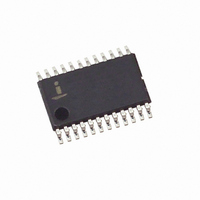
IC DC-DC CONVERTER 4CH 24-TSSOP

EL7584IR

Manufacturer Part Number
EL7584IR
Description
IC DC-DC CONVERTER 4CH 24-TSSOP
Manufacturer
Intersil
Datasheet

Specifications of EL7584IR

Applications
Converter, TFT, LCD
Voltage - Input
2 ~ 14 V
Number Of Outputs
2
Voltage - Output
5 ~ 17 V
Operating Temperature
-40°C ~ 85°C
Mounting Type
Surface Mount
Package / Case
24-TSSOP
Lead Free Status / RoHS Status
Contains lead / RoHS non-compliant

Available stocks

Company
Part Number
Manufacturer
Quantity
Price
Part Number:
EL7584IRZ
Manufacturer:
INTERSIL
Quantity:
20 000
Part Number:
EL7584IRZ-T13
Manufacturer:
INTERSIL
Quantity:
20 000
4-Channel DC/DC Converter
The EL7584 is a 4-channel DC/DC converter IC which is
designed primarily for use in TFT-LCD applications. The
boost converter has 2V to 14V input capability and provides
5V to 17V output, which powers the column drivers and
provides up to 370mA @ 15V. A pair of charge pump control
circuits provide outputs to allow the external generation of
V
respectively, each at up to 60mA for V
V
from 2V to 13V.
The EL7584 features adjustable switching frequency and on-
chip power sequence to simplify start-up operation. A
separate input is available to externally increase the default
delay of the positive charge pump. An over-temperature
feature is provided to allow the IC to be automatically
protected from excessive power dissipation.
The EL7584 is available in a 24-pin TSSOP package and is
specified for operation over the full -40°C to +85°C
temperature range.
Pinout
ON
COM
and V
buffer provides up to 50mA continuous output current
OFF
VDDB
DRVN
VDDN
VSSN
FBB
FBN
LX1
LX2
INC
supplies at 5V to 40V and 0V to -40V,
SS
EN
DP
10
12
11
1
2
3
4
5
6
7
8
9
(24-PIN TSSOP)
TOP VIEW
EL7584
®
1
Data Sheet
24
23
22
21
20
19
18
17
16
15
14
13
BOOST
VSSB
ROSC
VREF
PGND
PGND
VSSP
DRVP
VDDP
FBP
VSSC
VCOM
VDDC
Copyright © Intersil Americas Inc. 2003. All Rights Reserved. Elantec is a registered trademark of Elantec Semiconductor, Inc.
= 15V. The
1-888-INTERSIL or 321-724-7143
CAUTION: These devices are sensitive to electrostatic discharge; follow proper IC Handling Procedures.
Features
• TFT-LCD display supply
• 2V to 14V V
• 5V < V
• 2V < V
• 5V < V
• -40V < V
• V
• High frequency, small inductor DC/DC boost circuit
• Over 90% efficient DC/DC boost converter capability
• Built-in power-up sequence with adjustable V
• Adjustable frequency
• Adjustable soft-start
• Adjustable outputs
• Over-temperature protection
• Small parts count
• Pb-free available (RoHS compliant)
Applications
• TFT-LCD panels
• PDAs
Ordering Information
NOTE: Intersil Pb-free products employ special Pb-free material sets; molding
compounds/die attach materials and 100% matte tin plate termination finish, which are
RoHS compliant and compatible with both SnPb and Pb-free soldering operations.
Intersil Pb-free products are MSL classified at Pb-free peak reflow temperatures that
meet or exceed the Pb-free requirements of IPC/JEDEC J STD-020.
EL7584IR
EL7584IR-T7
EL7584IR-T13
EL7584IRZ
(See Note)
EL7584IRZ-T7
(See Note)
EL7584IRZ-
T13 (See Note)
- Boost regulator
- V
- V
- V
NUMBER
BOOST
PART
February 4, 2005
COM
ON
OFF
All other trademarks mentioned are the property of their respective owners.
BOOST
COM
ON
charge pump
charge pump
|
OFF
buffer
= 15V @ 370mA
Intersil (and design) is a registered trademark of Intersil Americas Inc.
< 40V
IN
< 13V
< 0V
24-Pin TSSOP
24-Pin TSSOP
24-Pin TSSOP
24-Pin TSSOP
24-Pin TSSOP
24-Pin TSSOP
< 17V
supply
PACKAGE
(Pb-free)
(Pb-free)
(Pb-free)
TAPE & REEL PKG. DWG. #
13”
13”
7”
7”
-
-
EL7584
FN7317.2
ON
MDP0044
MDP0044
MDP0044
MDP0044
MDP0044
MDP0044
delay

Related parts for EL7584IR

EL7584IR Summary of contents

Page 1

... EL7584IR EL7584IR-T7 VDDP EL7584IR-T13 FBP EL7584IRZ VSSC (See Note) EL7584IRZ-T7 VCOM (See Note) VDDC EL7584IRZ- T13 (See Note) NOTE: Intersil Pb-free products employ special Pb-free material sets; molding compounds/die attach materials and 100% matte tin plate termination finish, which are RoHS compliant and compatible with both SnPb and Pb-free soldering operations. ...

Page 2

Absolute Maximum Ratings ( Pin Voltage . . . . . . . . . . . . . . . . . . . . . . . . . . . . . . . . ...

Page 3

Electrical Specifications V = 3.3V PARAMETER DESCRIPTION POSITIVE REGULATED CHARGE PUMP (V Most positive V output depends on the magnitude of the V ON configuration (doubler or tripler) V Supply Input for Positive Charge Pump DDP IQ1(V ) ...

Page 4

Pin Descriptions I = Input Output Supply PIN NUMBER PIN NAME FBB VDDB 5 LX1 6 LX2 7 VSSN* 8 DRVN 9 VDDN 10 FBN INC 13 ...

Page 5

Typical Performance Curves 12V 80 15V =3. FREQ=1MHz 50 0 100 200 300 400 500 I (mA) OUT FIGURE 1. EFFICIENCY 12V 15V ...

Page 6

Typical Performance Curves f=675kHz, V =5.0V IN 1.5 1.0 0.5 0.0 -0.5 -1.0 18V 15V -1.5 0 100 200 300 400 I (mA) OUT FIGURE 7. LOAD REGULATION vs I f=1MHz, V =5.0V IN 1.5 1.0 0.5 0.0 -0.5 -1.0 ...

Page 7

Typical Performance Curves f(MHz)=1/(0.0118 R +0.378) OSC 1400 1200 1000 800 600 400 200 100 150 200 250 R (kΩ) OSC FIGURE 13 100K & 0.1µF DELAY NETWORK ON ENP, C 5V/DIV 10V/DIV ...

Page 8

Typical Performance Curves JEDEC JESD51-7 HIGH EFFECTIVE THERMAL CONDUCTIVITY TEST BOARD 1.4 1.2 1.176W 1 0.8 0.6 0.4 0 AMBIENT TEMPERATURE (°C) FIGURE 19. PACKAGE POWER DISSIPATION vs AMBIENT TEMPERATURE Functional Block Diagram FBB MAX_DUTY ...

Page 9

Applications Information The EL7584 is high efficiency multiple output power solution designed specifically for thin-film transistor (TFT) liquid crystal display (LCD) applications. The device contains one high current boost converter and two low power charge pumps (V and V ). ...

Page 10

The following table gives typical values: (Margins are considered 10%, 3%, 20%, 10%, and 15 and I , respectively LMT TABLE 1. MAXIMUM CONTINUOUS OUTPUT CURRENT V (V) V ...

Page 11

Single Stage Charge Pump V DDN 5V TO 17V 0.1µF R ONP DRVN C CPN V R OFF ONN C OUT2 V SSN 3.3µ FBN REF Positive Charge Pump Design Considerations A single stage charge ...

Page 12

Two-Stage Positive Charge Pump Circuit V DDP R ONP DRNP R ONN V SSP - + 1.265V The maximum V output voltage for N+1 stage charge pump is ≤ × × × max 2 V ...

Page 13

Two-Stage Negative Charge Pump Circuit V DDN R DRVN The maximum V output voltage for N+1 stage charge pump is: OFF ( ) ≥ × × max OFF OUT ...

Page 14

This means the active transconductance is: × × 2π 1µF 500kHz 3.14S = This high transconductance indicates why it is important to ...

Page 15

Typical Application Circuit R 2 110kΩ 13kΩ BOOST (12V@ 22µF 350mA) VIN 10µF GND V OFF 154kΩ 3.3µF **D 21 REFERENCE * MBRM120LT3 ** BAT54S *** ...

Page 16

... Accordingly, the reader is cautioned to verify that data sheets are current before placing orders. Information furnished by Intersil is believed to be accurate and reliable. However, no responsibility is assumed by Intersil or its subsidiaries for its use; nor for any infringements of patents or other rights of third parties which may result from its use ...

Related keywords