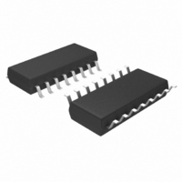
MIC9131BM Micrel Inc, MIC9131BM Datasheet - Page 13

MIC9131BM
Manufacturer Part Number
MIC9131BM
Description
IC CTRLR DC-DC PWM HV HS 16-SOIC
Manufacturer
Micrel Inc
Datasheet
1.MIC9131YM.pdf
(19 pages)
Specifications of MIC9131BM
Applications
Controller, Telecom
Voltage - Input
9 ~ 18 V
Number Of Outputs
1
Voltage - Output
4.7 ~ 5 V
Operating Temperature
-40°C ~ 125°C
Mounting Type
Surface Mount
Package / Case
16-SOIC (3.9mm Width)
Lead Free Status / RoHS Status
Contains lead / RoHS non-compliant
Available stocks
Company
Part Number
Manufacturer
Quantity
Price
cycle of the gate drive output increases until the error ampli-
fier takes control of the duty cycle. The soft start capacitor is
discharged by an internal MOSFET in the MIC9131.
The soft start circuit is activated by the following events:
Calculating the soft capacitor depends on many parameters
such as the current limit of the circuit input voltage, output
power and output loading. A starting value of capacitor should
be chosen and the value can be adjusted later in the design.
Recommended starting values of soft start capacitance is
typically 10nF to 100nF. Values below 1nF may be ineffective
in slowing the output voltage turn on time.
CPWR Current Limit Selection
This pin controls whether the soft start circuit is reset if the
voltage on the Isns pin exceeds the overcurrent threshold.
When the CPWR pin is high, an overcurrent condition at the
ISNS pin will terminate the on-time of the gate drive pulse and
discharge the soft start capacitor to 0V. This delay in start up
contributes to a reduction in the average output current during
an overcurrent or short circuit condition. A smaller MOSFET
may be used since the power dissipation in the MOSFET is
minimized under short circuit or overcurrent conditions.
If the CPWR pin is low an overcurrent or short circuit condi-
tions will not trip the soft start circuit. The pulse-by-pulse
current limit, inherent in current mode control, provides a
“brick wall” or constant current limit. With the power supply
operating in this mode, a smaller soft start capacitor can be
used to increase the turn on speed of the supply.
If the CPWR in is held low during the initial turn on at power
up and then raised high, the power supply can maximize
the turn-on time at start up and still provide a high level of
overcurrent and short circuit protection. The circuit shown
in Figure 7 performs this function.
MOSFET Gate Drive Output
The MIC9131 has the capability to directly drive the gate of
a MOSFET. The output driver consists of a complimentary
P-channel and N-channel pair. The typical switching time
August 2006
MIC9131
1. Line undervoltage pin less than the 1.21V threshold
2. V
3. The current limit comparator threshold is exceeded.
4. A low level on the enable pin.
This can be disabled with a low level on the CPWR
pin.
CC
becomes less than the pre-regulator voltage turn
D1
C1
R1
Figure 7
V
CPWR
REF
MIC9131
AGND
off threshold.
13
of the output is dependent on the IC supply voltage and the
gate charge required to turn the MOSFET on and off.
A resistor placed in series with the gate drive output attenu-
ates ringing in the etch connection between the MIC9131
and the MOSFET. Figure 8 shows a single resistor in series
between the driver output and the gate of the MOSFET. The
zener value should be greater than the gate drive voltage
to prevent excessive power dissipation, but less than the
maximum gate to source voltage rating.
The circuitry shown in figure 9 allow different rise and fall
times. R1 and the input capacitance of the MOSFET de-
termine the rise-time of the gate voltage and therefore the
turn-on time of the MOSFET. The diode, D1 is reversed
biased, which removes R2 from the circuit. At turn-off, D1
is forward biased and the parallel combination of R1 and R2
controls the turn-off time of the MOSFET. The turn on-time
is slower, which reduces switching noise and ringing during
turn-on. The turn-off time is faster, which minimizes switching
losses during turn-off and improves efficiency. If the turn-on
time is to be faster than the turn-off time, the diode should
be reversed.
A gate drive transformer is used where an increase in drive
voltage, isolation and/or voltage level shifting are required.
Gate drive transformers can have multiple windings and drive
multiple MOSFETs, including MOSFETs that require a drive
signal 180°C out of phase with the ICs drive signal.
Figure 10 shows a gate drive transformer circuit. The ca-
pacitor, C1 removes DC from the drive circuit and prevents
transformer saturation. R1 provides damping to eliminate
ringing in the circuit. R1 is usually in the 5 to 20Ω range,
depending on the amount of damping necessary. D1 and
D2 form a clamp circuit, which prevents the voltage from
exceeding the V
the diodes may be removed R2 is used to allow the trans-
former to reset properly.
Gate Drive
GMAX
Output
GND
Gate Drive
level. If the gate drive is well damped,
Output
GND
Figure 8
Figure 9
R2
D1
R1
M9999-080206
Micrel, Inc.


