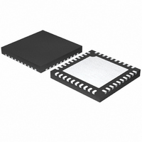
MAX1567ETL+ Maxim Integrated Products, MAX1567ETL+ Datasheet - Page 32

MAX1567ETL+
Manufacturer Part Number
MAX1567ETL+
Description
IC DGTL CAM PWR-SUP 6CH 40TQFN
Manufacturer
Maxim Integrated Products
Datasheet
1.MAX1567ETLT.pdf
(35 pages)
Specifications of MAX1567ETL+
Applications
Controller, Digital Camera
Voltage - Input
0.7 ~ 5.5 V
Number Of Outputs
7
Voltage - Output
1.25 ~ 5 V
Operating Temperature
-40°C ~ 85°C
Mounting Type
Surface Mount
Package / Case
40-TQFN Exposed Pad
Lead Free Status / RoHS Status
Lead free / RoHS Compliant
Six-Channel, High-Efficiency, Digital
Camera Power Supplies
In that case:
Place:
Or, reduce the inductor value for discontinuous operation.
Figures 1, 2, and 3 show connections for AA and Li+
battery arrangements. Figures 7–13 show various con-
nections for the AUX1, 2, and 3 controllers. Figures 15,
16, and 17 show various connections for the SDOK,
AUX1OK, and SCF outputs.
In this connection, the main converter is operated as a
step-down (SUSD = GND) and is powered from PVSU.
This provides boost-buck operation for the main 3.3V
output so a regulated output is maintained over the Li+
2.7V to 4.2V cell voltage range. The compound efficien-
cy from the battery to the 3.3V output reaches 90%.
The step-down 1.8V (core) output is powered directly
from V
The CCD and LCD voltages are generated with a trans-
formerless design. AUX1 generates +15V for CCD posi-
tive and LCD bias. The MAX1567 AUX2 inverter
generates -7.5V for negative CCD bias. The AUX3 con-
troller generates a regulated current for a series net-
work of four white LEDs that backlight the LCD.
Figure 2 is optimized for 2-cell AA inputs (1.5V to 3.7V)
by connecting the step-down input (PVSD) to the main
output (PVM). The main 3.3V output operates directly
from the battery as a step-up (SUSD = PVSD). The 1.8V
core output now operates as a boost-buck with efficien-
cy up to 90%. The rest of the circuit is unchanged from
Figure 1.
The MAX1566/MAX1567 can also allow either 1-cell Li+
or 2 AA cells to power the same design. If the step-
down and main inputs are both connected to PVSU,
then both the 3.3V and 1.8V outputs operate as boost-
buck converters. There is an efficiency penalty com-
pared to stepping down VSD directly from the battery,
but that is not possible with a 1.5V input.
32
1 / (2π x R
Figure 1. Typical Operating Circuit for One Li+ Cell
Figure 2. Typical Operating Circuit for 2 AA Cells
Figure 3. Typical Operating Circuit for 2 AA Cells
______________________________________________________________________________________
BATT
.
C
(V
x C
REF
C
Applications Information
C
R
C
C
= (V
+ |V
) = 1 / (2π x R
= R
Typical Operating Circuits
IN
OUT
LOAD
/ V
|)] [g
RAMP
x C
M
LOAD
OUT
) [V
/ (2π x f
REF
/ C
x C
C
/
C
and 1-Cell Li+
OUT
)]
), so that
Furthermore, the cascaded boost-buck efficiency com-
pares favorably with other boost-buck techniques.
Any AUX channel (except for the AUX2 inverter on the
MAX1567) can be used for a wide variety of step-up
applications. These include generating 5V or some
other voltage for motor or actuator drive, generating
15V or a similar voltage for LCD bias, or generating a
step-up current source to efficiently drive a series array
of white LEDs to display backlighting. Figures 7 and 8
show examples of these applications.
Some applications require multiple voltages from a sin-
gle converter channel. This is often the case when gen-
erating voltages for CCD bias or LCD power. Figure 9
shows a two-output flyback configuration with an AUX
channel. The controller drives an external MOSFET that
switches the transformer primary. Two transformer sec-
ondaries generate the output voltages. Only one posi-
tive output voltage can be fed back, so the other
voltages are set by the turns-ratio of the transformer
secondaries. The load stability of the other secondary
voltages depends on transformer leakage inductance
and winding resistance. Voltage regulation is best
when the load on the secondary that is not fed back is
small compared to the load on the one that is fed back.
Regulation also improves if the load-current range is
limited. Consult the transformer manufacturer for the
proper design for a given application.
On the MAX1567, AUX2 is set up to drive an external P-
channel MOSFET in an inverting configuration. DL2 drives
low to turn on the MOSFET, and FB2 has inverted polarity
and a 0V threshold. This is useful for generating negative
CCD bias without a transformer, particularly with high
pixel-count cameras that have a greater negative CCD
load current. Figure 10 shows an example circuit.
Another method of producing bipolar output voltages
without a transformer is with an AUX controller and a
charge-pump circuit, as shown in Figure 11. When MOS-
FET Q1 turns off, the voltage at its drain rises to supply
current to V
voltage V
C1 discharges through D3, thereby charging C3 to V
minus the drop across D3 to create roughly the same
voltage as V
Transformerless Inverter for Negative CCD
Boost with Charge Pump for Positive and
LED, LCD, and Other Boost Applications
OUT+
OUT+
OUT+
Multiple-Output Flyback Circuits
through D1. When the MOSFET turns on,
. At the same time, C1 charges to the
at V
OUT-
, but with inverted polarity.
Bias (AUX2, MAX1567)
Negative Outputs
OUT
-


