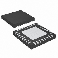
MAX1518BETJ+T Maxim Integrated Products, MAX1518BETJ+T Datasheet

MAX1518BETJ+T
Specifications of MAX1518BETJ+T
Related parts for MAX1518BETJ+T
MAX1518BETJ+T Summary of contents
Page 1
... PIN-PACKAGE RANGE -40°C to MAX1518BETJ 32 Thi n QFN +100°C ________________________________________________________________ Maxim Integrated Products For pricing, delivery, and ordering information, please contact Maxim/Dallas Direct! at 1-888-629-4642, or visit Maxim’s website at www.maxim-ic.com. TFT-LCD DC-DC Converter with Operational Amplifiers ♦ 2.6V to 6.5V Input Supply Range ♦ 1.2MHz Current-Mode Step-Up Regulator Fast Transient Response to Pulsed Load High-Accuracy Output Voltage (1 ...
Page 2
TFT-LCD DC-DC Converter with Operational Amplifiers ABSOLUTE MAXIMUM RATINGS IN, CTL to AGND ......................................................-0.3V to +7V COMP, FB, FBP, FBN, DEL, REF to AGND ....-0. PGND, BGND to AGND ......................................................±0. PGND ............................................................-0.3V to +14V SUP to ...
Page 3
ELECTRICAL CHARACTERISTICS (continued 3V 8V, PGND = AGND = BGND = SUP wise noted.) PARAMETER SYMBOL LX On-Resistance R LX Leakage Current LX Current Limit Current-Sense Transconductance Soft-Start Period Soft-Start Step Size OPERATIONAL ...
Page 4
TFT-LCD DC-DC Converter with Operational Amplifiers ELECTRICAL CHARACTERISTICS (continued 3V 8V, PGND = AGND = BGND = SUP wise noted.) FBP Line (IN) Regulation Error DRVP Sink Current I DRVP DRVP Off-Leakage Current ...
Page 5
ELECTRICAL CHARACTERISTICS ( 8V, PGND = AGND = BGND = SUP PARAMETER SYMBOL IN Supply Range IN Undervoltage-Lockout Threshold IN Quiescent Current REF Output Voltage MAIN STEP-UP REGULATOR Output Voltage Range Operating Frequency ...
Page 6
TFT-LCD DC-DC Converter with Operational Amplifiers ELECTRICAL CHARACTERISTICS (continued 3V 8V, PGND = AGND = BGND = SUP FBP Effective Load-Regulation Error (Transconductance) FBP Line (IN) Regulation Error DRVP Sink Current I DRVP ...
Page 7
Figure 5V 13V MAIN unless otherwise noted.) STEP-UP EFFICIENCY vs. LOAD CURRENT 100 13V OUT ...
Page 8
TFT-LCD DC-DC Converter with Operational Amplifiers (Circuit of Figure 5V 13V MAIN unless otherwise noted.) GATE-ON REGULATOR LINE REGULATION 0.2 0 -0.2 -0.4 -0 23.5V GON -0 20mA GON ...
Page 9
Figure 5V 13V MAIN unless otherwise noted.) OPERATIONAL-AMPLIFIER LOAD-TRANSIENT RESPONSE MAX1518B toc15 0V +50mA 0 -50mA 400ns/div A: OUTPUT VOLTAGE, 1V/div, AC-COUPLED B: OUTPUT CURRENT, 50mA/div PIN NAME Switch Input. Source ...
Page 10
TFT-LCD DC-DC Converter with Operational Amplifiers PIN NAME 17 OUT4 Operational-Amplifier 4 Output 18 POS5 Operational-Amplifier 5 Noninverting Input 19 NEG5 Operational-Amplifier 5 Inverting Input 20 OUT5 Operational-Amplifier 5 Output n-Channel Power MOSFET Drain and Switching Node. Connect the inductor ...
Page 11
Typical Operating Circuit The MAX1518B Typical Operating Circuit (Figure complete power-supply system for TFT LCDs. The cir- cuit generates a +13V source-driver supply and +24V and -8V gate-driver supplies. The input voltage range for the IC is ...
Page 12
TFT-LCD DC-DC Converter with Operational Amplifiers V IN 4.5V TO 5.5V C1 22µF R10 10Ω C18 0.1µF 180kΩ 220µF LX 0.1µF 6.8kΩ 0.1µ 332kΩ GOFF -8V/50mA 0.22µF R8 40.2kΩ 1% 0.22µF 0.033µF TO VCOM BACKPLANE ...
Page 13
V IN Figure 2. MAX1518B Functional Diagram ______________________________________________________________________________________ TFT-LCD DC-DC Converter with Operational Amplifiers STEP-UP CONTROLLER PGND COMP AGND MAX1518B DRVP GATE-ON CONTROLLER FBP SRC DEL COM SWITCH CONTROL CTL DRN DRVN GATE-OFF CONTROLLER SUP ...
Page 14
TFT-LCD DC-DC Converter with Operational Amplifiers CLOCK OSCILLATOR TO FAULT LATCH Figure 3. Step-Up Regulator Functional Diagram This discharge condition forces the current through the inductor to ramp back down, transferring the energy stored in the magnetic field to the ...
Page 15
V MAIN DRVP NPN CASCODE TRANSISTOR MAX1518B FBP Figure 4. Using Cascoded npn for Charge-Pump Output Voltages > 28V Gate-Off Linear-Regulator Controller, REG N The gate-off linear-regulator controller (REG analog gain block with an open-drain p-channel output. ...
Page 16
TFT-LCD DC-DC Converter with Operational Amplifiers Undervoltage Lockout (UVLO) The undervoltage-lockout (UVLO) circuit compares the input voltage at IN with the UVLO threshold (2.5V rising, 2.30V falling, typ) to ensure the input voltage is high enough for reliable operation. The ...
Page 17
IN 5µA DEL REF CTL Figure 7. Switch-Control Block During steady-state operation, if the output of the main regulator or any of the linear-regulator outputs does not exceed its respective fault-detection threshold, the MAX1518B activates an internal fault timer. If ...
Page 18
TFT-LCD DC-DC Converter with Operational Amplifiers Design Procedure Main Step-Up Regulator The minimum inductance value, peak current rating, and series resistance are factors to consider when selecting the inductor. These factors influence the con- verter’s efficiency, maximum output load capability, ...
Page 19
Output-Capacitor Selection The total output voltage ripple has two components: the capacitive ripple caused by the charging and discharg- ing of the output capacitance, and the ohmic ripple due to the capacitor’s equivalent series resistance (ESR ...
Page 20
TFT-LCD DC-DC Converter with Operational Amplifiers STEP-UP CONTROLLER PGND MAX1518B Figure 8. Operation with Output Voltages >13V Using Cascoded MOSFET The number of negative charge-pump stages is given by: − GOFF DROPOUT = ...
Page 21
POSITIVE CHARGE-PUMP OUTPUT VOLTAGE vs 3-STAGE CHARGE PUMP 2-STAGE CHARGE PUMP 1-STAGE CHARGE PUMP (V) MAIN Figure 9. Positive Charge-Pump Output ...
Page 22
TFT-LCD DC-DC Converter with Operational Amplifiers The transconductance amplifier regulates the output voltage by controlling the pass transistor’s base cur- rent. The total DC loop gain is approximately: × BIAS ≅ × ...
Page 23
Applications Information Power Dissipation An IC’s maximum power dissipation depends on the thermal resistance from the die to the ambient environ- ment and the ambient temperature. The thermal resis- tance depends on the IC package, PC board copper area, other ...
Page 24
TFT-LCD DC-DC Converter with Operational Amplifiers TOP VIEW AGND PGND OUT1 NEG1 POS1 OUT2 24 ______________________________________________________________________________________ SRC 1 REF MAX1518B ...
Page 25
... Maxim cannot assume responsibility for use of any circuitry other than circuitry entirely embodied in a Maxim product. No circuit patent licenses are implied. Maxim reserves the right to change the circuitry and specifications without notice at any time. Maxim Integrated Products, 120 San Gabriel Drive, Sunnyvale, CA 94086 408-737-7600 ____________________ 25 © 2005 Maxim Integrated Products ...


