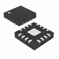
MAX8723ETE+T Maxim Integrated Products, MAX8723ETE+T Datasheet - Page 13

MAX8723ETE+T
Manufacturer Part Number
MAX8723ETE+T
Description
IC REG FOR LCD DISPLAY 16-TQFN
Manufacturer
Maxim Integrated Products
Specifications of MAX8723ETE+T
Applications
Converter, LCD
Voltage - Input
6 ~ 13.2 V
Number Of Outputs
1
Voltage - Output
3.3V, 2 ~ 3.6 V
Operating Temperature
-40°C ~ 85°C
Mounting Type
Surface Mount
Package / Case
16-TQFN Exposed Pad
Lead Free Status / RoHS Status
Lead free / RoHS Compliant
The linear regulator output VL is enabled when the
MAX8723 input voltage rises high enough to lift VL
above its undervoltage lockout (UVLO) threshold. When
the reference voltage (REF) is above its UVLO thresh-
old and SHDN is logic-high, the step-down regulator
starts up. At this time, an internal reference voltage
steps from zero to REF, making the output of the step-
down converter gradually increase to its regulation
point. This soft-start takes about 1.7ms and prevents
large inrush currents. The FB undervoltage fault detec-
tion is blanked during the soft-start and is enabled after
the step-down regulator reaches regulation.
The MAX8723 step-down regulator is disabled when
SHDN is logic-low or when the fault protection latch is set.
The MAX8723 monitors OUT (fixed-output mode) or FB
(adjustable-output mode) for undervoltage conditions.
During steady-state operation, if the voltage drops below
80% (typ) of the nominal regulation point, the MAX8723
activates an internal fault timer. If the fault persists longer
than the fault timer duration (50ms, typ), the MAX8723
sets a fault latch, shutting down step-down regulator out-
put. The linear regulator output VL and reference output
REF remain active during output undervoltage faults.
Once the fault condition is removed, toggle SHDN or
cycle the input voltage to clear the fault latch and restart
the step-down switching regulator.
The thermal-overload protection prevents excessive
power dissipation from overheating the MAX8723. When
the junction temperature exceeds T
sensor immediately activates a fault-protection circuit,
which shuts down OUT, allowing the device to cool down.
Once the device cools down by approximately 15°C, the
MAX8723 automatically restarts the step-down regulator.
For continuous operation, do not exceed the absolute
maximum junction temperature rating of T
The reference output is nominally 2V, and can source
at least 50µA (see Typical Operating Characteristics).
VCC is the supply input of the internal reference block.
Bypass REF with a 0.22µF ceramic capacitor connect-
ed between REF and GND.
The MAX8723 includes an internal linear regulator (VL).
INL is the supply input of the linear regulator and the
input voltage range is between 6V and 13.2V. The VL
output voltage is set to 5V. VL powers the internal MOS-
FET driver circuit, the external MOSFET driver circuit (if
Thermal-Overload Protection
______________________________________________________________________________________
Power Sequence Control
Low-Cost, Internal-Switch, Step-Down
Reference Voltage (REF)
Linear Regulator (VL)
J
Fault Protection
= +160°C, a thermal
J
= +150°C.
Regulator for LCD Displays
used), the PWM controller, and logic circuits. Through
VCC, VL powers the internal reference, current-limit cir-
cuitry, and other sensitive blocks.
Bypass VL with at least a 1µF ceramic capacitor. VL can
supply at least 25mA to external loads when bypassed
with a 2.2µF ceramic capacitor. VL can supply power for
on/off monitoring and remote-control receiver circuitry.
Three key inductor parameters must be specified:
inductance value (L), peak current (I
resistance (R
constant, LIR, which is the ratio of peak-to-peak induc-
tor ripple current to DC load current. A higher LIR value
allows smaller inductance, but results in higher losses
and higher ripple. A good compromise between size
and losses is typically found at a 30% ripple current-to-
load current ratio (LIR = 0.3), which corresponds to a
peak inductor current 1.15 times the DC load current:
where I
the switching frequency f
tied to AGND, 1MHz when FSEL is tied to V
500kHz when FSEL is tied to REF. The exact inductor
value is not critical and can be adjusted to make trade-
offs among size, cost, and efficiency. Lower inductor
values minimize size and cost, but they also increase
the output ripple and reduce the efficiency due to high-
er peak currents. On the other hand, higher inductor
values reduce output ripple and improve efficiency, but
at some point resistive losses due to extra turns of wire
exceed the benefit gained from lower AC current levels.
The inductor’s saturation current must exceed the peak
inductor current. The peak current can be calculated by:
The inductor’s DC resistance should be low for good
efficiency. Find a low-loss inductor having the lowest
possible DC resistance that fits in the allotted dimen-
sions. Ferrite cores are often the best choice. Shielded-
core geometries help keep noise, EMI, and switching
waveform jitter low.
OUT(MAX)
I
I
OUT RIPPLE
OUT PEAK
L
_
_
DC
=
V
). The following equation includes a
IN
is the maximum DC load current, and
V
×
=
OUT
f
=
I
SW
OUT MAX
V
OUT
×
×
SW
(
Design Procedure
(
I
f
OUT MAX
SW
V
IN
×
is 1.5MHz when FSEL is
)
(
× ×
Inductor Selection
−
(
V
+
L V
V
IN
OUT
I
OUT RIPPLE
−
)
V
IN
×
OUT
)
_
LIR
PEAK
2
)
), and DC
CC
, and
13


