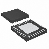
MAX1584ETJ+T Maxim Integrated Products, MAX1584ETJ+T Datasheet - Page 19

MAX1584ETJ+T
Manufacturer Part Number
MAX1584ETJ+T
Description
IC DGTL CAM PWR-SUP 5CH 32TQFN
Manufacturer
Maxim Integrated Products
Datasheet
1.MAX1585ETJ.pdf
(29 pages)
Specifications of MAX1584ETJ+T
Applications
Controller, Digital Camera
Voltage - Input
0.7 ~ 5.5 V
Number Of Outputs
5
Voltage - Output
1.25 ~ 5.5 V
Operating Temperature
-40°C ~ 85°C
Mounting Type
Surface Mount
Package / Case
32-TQFN Exposed Pad
Lead Free Status / RoHS Status
Lead free / RoHS Compliant
iary converters and cannot be activated until PVSU is in
regulation. For automatic startup, connect ON_ to PVSU
or a logic level greater than 1.6V.
Choose a switching frequency to optimize external
component size or circuit efficiency for the particular
application. Typically, switching frequencies between
400kHz and 500kHz offer a good balance between
component size and circuit efficiency—higher frequen-
cies generally allow smaller components, and lower fre-
quencies give better conversion efficiency. The
switching frequency is set with an external timing resistor
(R
cycle, the timing capacitor charges through the resistor
until it reaches V
The capacitor voltage then decays to zero over time t
= 150ns. The oscillator frequency is as follows:
f
between 22pF and 470pF. Determine R
See the Typical Operating Characteristics section for
f
The MAX1584/MAX1585 step-up and step-down con-
verters and the AUX1 controllers have resistor-
adjustable output voltages. When setting the voltage for
all channels except AUX2 on the MAX1585, connect a
resistive voltage-divider from the output voltage to the
corresponding FB_ input. The FB_ input bias current is
less than 100nA, so choose the low-side (FB_-to-GND)
resistor (R
high-side (output-to-FB_) resistor (R
AUX2 is an inverter on the MAX1585, so the FB2
threshold on the MAX1585 is 0V. To set the MAX1585
AUX2 negative output voltage, connect a resistive volt-
age-divider from the negative output to the FB2 input,
and then to REF. The FB2 input bias current is less than
100nA, so choose the REF-side (FB2-to-REF) resistor
(R
(negative output-to-FB2) resistor:
OSC
OSC
REF
OSC
R
vs. R
can be set from 100kHz to 1MHz. Choose C
) to be 100kΩ or less. Then calculate the top-side
OSC
) and capacitor (C
t
1
= -R
OSC
L
R
= (150ns - 1 / f
) to be 100kΩ or less. Then calculate the
TOP
Setting the Switching Frequency
V
OSC
R
PVSU
using different values of C
H
REF
= R
= R
______________________________________________________________________________________
f
x C
OSC
])
. The charge time, t
REF
L
OSC
[(V
= 1 / (t
Setting Output Voltages
(-V
OSC
OUT
OSC
x l
Design Procedure
OUT(AUX2)
5-Channel Slim DSC Power Supplies
n
) / (C
). At the beginning of a
(1 - 1.25 / V
1
/ 1.25) - 1]
+ t
OSC
2
H
)
):
/ 1.25)
OSC
1
x l
, is as follows:
OSC
n
PVSU
[1 - 1.25
:
.
)
OSC
2
The input capacitor in a DC-DC converter reduces cur-
rent peaks drawn from the battery or other input power
source and reduces switching noise in the controller.
The impedance of the input capacitor at the switching
frequency should be less than that of the input source
so high-frequency switching currents do not pass
through the input source.
The output capacitor keeps output ripple small and
ensures control-loop stability. The output capacitor
must also have low impedance at the switching fre-
quency. Ceramic, polymer, and tantalum capacitors
are suitable, with ceramic exhibiting the lowest ESR
and high-frequency impedance.
Output ripple with a ceramic output capacitor is
approximately:
If the capacitor has significant ESR, the output ripple
component due to capacitor ESR is:
Output capacitor specifics are also discussed in each
converter’s Compensation section.
The external components required for the step-up are
an inductor, an input and output filter capacitor, and a
compensation RC.
The inductor is typically selected to operate with contin-
uous current for best efficiency. An exception might be
if the step-up ratio, (V
D
of 80%.
When using the step-up channel to boost from a low
input voltage, loaded startup is aided by connecting a
Schottky diode from the battery to PVSU. See the
Minimum Startup Voltage vs. Load Current graph in the
Typical Operating Characteristics section.
In most step-up designs, a reasonable inductor value
(L
which sets continuous peak-to-peak inductor current at
half the DC inductor current:
where D is the duty factor given by:
Given L
rent is 0.5 x I
as follows:
MAX
IDEAL
L
), where D
IDEAL
V
) can be derived from the following equation,
IDEAL
RIPPLE
General Filter-Capacitor Selection
= [2V
V
, the consistent peak-to-peak inductor cur-
OUT
RIPPLE(ESR)
= I
MAX
Step-Up Component Selection
IN(MAX)
L(PEAK)
/ (1 - D). The peak inductor current is
D = 1 - (V
is the maximum PWM duty factor
OUT
x D(1 - D)] / (I
[1 / (2π x f
= I
/ V
IN
L(PEAK)
IN
/ V
), is greater than 1 / (1 -
OUT
OSC
)
x ESR
Step-Up Inductor
OUT
x C
OUT
x f
OSC
)]
)
19


