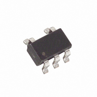
MAX870EUK+T Maxim Integrated Products, MAX870EUK+T Datasheet - Page 6

MAX870EUK+T
Manufacturer Part Number
MAX870EUK+T
Description
IC VOLT INVERT SW CAP SOT23-5
Manufacturer
Maxim Integrated Products
Datasheet
1.MAX871EUKT.pdf
(8 pages)
Specifications of MAX870EUK+T
Applications
Charge Pump, LCD
Voltage - Input
1.4 ~ 5.5 V
Number Of Outputs
1
Voltage - Output
-1.4 ~ 5.5 V
Operating Temperature
0°C ~ 85°C
Mounting Type
Surface Mount
Package / Case
SOT-23-5, SC-74A, SOT-25
Function
Inverting
Output Voltage
- 1.4 V to - 5.5 V
Output Current
25 mA
Maximum Operating Temperature
+ 85 C
Minimum Operating Temperature
- 40 C
Mounting Style
SMD/SMT
Lead Free Status / RoHS Status
Lead free / RoHS Compliant
Switched-Capacitor Voltage Inverters
Increasing the flying capacitor’s size reduces the output
resistance. Small C1 values increase the output resis-
tance. Above a certain point, increasing C1’s capaci-
tance has a negligible effect, because the output
resistance becomes dominated by the internal switch
resistance and capacitor ESR.
Increasing the output capacitor’s size reduces the output
ripple voltage. Decreasing its ESR reduces both output
resistance and ripple. Smaller capacitance values can
be used with light loads if higher output ripple can be
tolerated. Use the following equation to calculate the
peak-to-peak ripple:
Bypass the incoming supply to reduce its AC impedance
and the impact of the MAX870/MAX871’s switching
noise. The recommended bypassing depends on the cir-
cuit configuration and on where the load is connected.
When the inverter is loaded from OUT to GND, current
from the supply switches between 2 x I
Table 1. Low-ESR Capacitor Manufacturers
Table 2. Capacitor Selection for Minimum Output Resistance or Capacitor Size
6
Surface-Mount
Tantalum
Surface-Mount
Ceramic
_______________________________________________________________________________________
PRODUCTION
V
RIPPLE
METHOD
MAX870
MAX871
PART
=
f
OSC
I
OUT
x C2
AVX
Matsuo
Sprague
AVX
Matsuo
+ 2
MANUFACTURER
x I
Input Bypass Capacitor
125kHz
500kHz
Output Capacitor (C2)
OUT
f
Flying Capacitor (C1)
OSC
x ESR
OUT
C
2
and zero.
TPS series
267 series
593D, 595D series
X7R
X7R
CAPACITORS TO MINIMIZE
OUTPUT RESISTANCE
SERIES
(R
O
C1 = C2
= 23Ω, TYP)
Therefore, use a large bypass capacitor (e.g., equal to
the value of C1) if the supply has a high AC impedance.
When the inverter is loaded from IN to OUT, the circuit
draws 2 x I
spikes. A 0.1µF bypass capacitor is sufficient.
The most common application for these devices is a
charge-pump voltage inverter (Figure 1). This application
requires only two external components—capacitors C1
and C2—plus a bypass capacitor, if necessary. Refer to
the Capacitor Selection section for suggested capacitor
types.
Two devices can be cascaded to produce an even
larger negative voltage (Figure 4). The unloaded output
voltage is normally -2 x V
by the output resistance of the first device multiplied by
the quiescent current of the second. When cascading
more than two devices, the output resistance rises dra-
matically. For applications requiring larger negative
voltages, see the MAX864 and MAX865 data sheets.
The maximum load current and startup current of the
n th cascaded circuit must not exceed the maximum
output current capability of the (n-1) th circuit to ensure
proper stability.
0.33µF
1µF
(803) 946-0690
(714) 969-2491
(603) 224-1961
(803) 946-0690
(714) 969-2491
OUT
constantly, except for short switching
PHONE
CAPACITORS TO MINIMIZE SIZE
IN
, but this is reduced slightly
(R
Cascading Devices
O
(803) 626-3123
(714) 960-6492
(603) 224-1430
(803) 626-3123
(714) 960-6492
C1 = C2
Voltage Inverter
= 40Ω, TYP)
0.33µF
0.1µF
FAX


