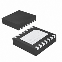
MAX8614BETD+T Maxim Integrated Products, MAX8614BETD+T Datasheet - Page 10

MAX8614BETD+T
Manufacturer Part Number
MAX8614BETD+T
Description
IC DC-DC CONV DL CCD 14TDFN
Manufacturer
Maxim Integrated Products
Datasheet
1.MAX8614AETDT.pdf
(15 pages)
Specifications of MAX8614BETD+T
Applications
Converter, CCD
Voltage - Input
2.7 ~ 5.5 V
Number Of Outputs
2
Voltage - Output
Adjustable up to 24V, Adjustable down to -10V
Operating Temperature
0°C ~ 85°C
Mounting Type
Surface Mount
Package / Case
14-TDFN Exposed Pad
Lead Free Status / RoHS Status
Lead free / RoHS Compliant
The inverter generates output voltages down to -16V
below V
diode allow conversion efficiencies as high as 85%.
Both converters use a fixed-frequency, PWM current-
mode control-scheme. The heart of the current-mode
PWM controllers is a comparator that compares the
error-amp voltage-feedback signal against the sum of
the amplified current-sense signal and a slope-com-
pensation ramp. At the beginning of each clock cycle,
the internal power switch turns on until the PWM com-
parator trips. During this time the current in the inductor
ramps up, storing energy in the inductor’s magnetic
field. When the power switch turns off, the inductor
releases the stored energy while the current ramps
down, providing current to the output.
The MAX8614A/MAX8614B have robust fault and over-
load protection. After power-up the device is set to
detect an out-of-regulation state that could be caused by
an overload or short condition at either output. If either
output remains in overload for more than 100ms, both
converters turn off and the FLT flag asserts low. During a
short-circuit condition longer than 100ms on the positive
output, foldback current limit protects the output. During
a short-circuit condition longer than 100ms on the nega-
tive output, both converters turn off and the FLT flag
asserts low. The converters then remain off until the
device is reinitialized by resetting the controller.
The MAX8614A/MAX8614B also have thermal shutdown.
When the device temperature reaches +170°C (typ) the
device shuts down. When it cools down by 20°C (typ),
the converters turn on.
Applying a high logic-level signal to ONBST/ONINV
turns on the converters using the soft-start and power-
on sequencing described below. Pulling ONBST/
ONINV low puts the IC in shutdown mode, turning off
the internal circuitry. When ONBST/ONINV goes high
(or if power is applied with ONBST/ONINV high), the
power-on sequence is set by SEQ. In shutdown, the
device consumes only 0.1µA and both output loads are
disconnected from the input supply.
The step-up converter and inverter in the MAX8614A/
MAX8614B feature soft-start to limit inrush current and
minimize battery loading at startup. This is accom-
plished by ramping the reference voltage at the input of
each error amplifier. The step-up reference is ramped
Dual-Output (+ and -) DC-DC
Converters for CCD
10
______________________________________________________________________________________
CC
. An internal power switch and external catch
Soft-Start and Inrush Current
Enable (ONBST/ONINV)
Fault Protection
Control Scheme
Inverter
from 0 to 1V (where 1V is the desired feedback voltage
for the step-up converter) while the inverter reference is
ramped down from 1.25V to 0 (where 0 is the desired
feedback voltage for the inverter).
During startup, the step-up converter True-Shutdown
load switch turns on before the step-up-converter refer-
ence voltage is ramped up. This effectively limits inrush
current peaks to below 500mA during startup.
The MAX8614A/MAX8614B feature undervoltage-lock-
out (UVLO) circuitry, which prevents circuit operation
and MOSFET switching when AV
UVLO threshold (2.55V, typ). The UVLO comparator
has 25mV of hysteresis to eliminate chatter due to the
source supply output impedance.
The MAX8614A/MAX8614B have pin-selectable inter-
nally programmed power-on sequencing. This
sequencing covers all typical sequencing options
required by CCD imagers.
When SEQ = 0, power-on sequence can be indepen-
dently controlled by ONINV and ONBST. When SEQ =
0 and ONINV and ONBST are pulled high, both outputs
reach regulation simultaneously. The inverter is held off
while the step-up True-Shutdown switch slowly turns on
to pull PVP to V
drop below V
voltage, the step-up and the inverter then ramp their
respective references over a period of 7ms. This brings
the two outputs into regulation at approximately the
same time.
When SEQ = 1 and ONBST and ONINV are pulled high,
the step-up output powers on first. The inverter is held
off until the step-up completes its entire soft-start cycle
and the positive output is in regulation. Then the inverter
starts its soft-start cycle and achieves regulation in
about 7ms.
The MAX8614A/MAX8614B completely disconnect the
loads from the input when in shutdown mode. In most
step-up converters the external rectifying diode and
inductor form a DC current path from the battery to the
output. This can drain the battery even in shutdown if a
load is connected at the step-up converter output. The
MAX8614A/MAX8614B have an internal switch between
the input V
switch turns off in shutdown there is no DC path from
the input to the output of the step-up converter. This
load disconnect is referred to as “True Shutdown.” At
CC
CC
and the inductor node, PVP. When this
CC
. Once the step-up output reaches this
Undervoltage Lockout (UVLO)
. The positive output rises to a diode
Power-On Sequencing (SEQ)
CC
True Shutdown
is less than the


