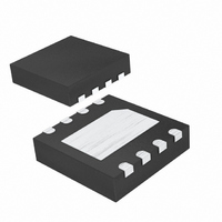
MAX8719ETA+T Maxim Integrated Products, MAX8719ETA+T Datasheet - Page 9

MAX8719ETA+T
Manufacturer Part Number
MAX8719ETA+T
Description
IC REG LINEAR LP HV 8-TDFN
Manufacturer
Maxim Integrated Products
Datasheet
1.MAX8719ETAT.pdf
(10 pages)
Specifications of MAX8719ETA+T
Applications
Converter, Notebook Computer
Voltage - Input
4 ~ 28 V
Number Of Outputs
1
Voltage - Output
1.24 ~ 28 V
Operating Temperature
0°C ~ 85°C
Mounting Type
Surface Mount
Package / Case
8-TDFN Exposed Pad
Polarity
Positive
Input Voltage Max
28 V
Output Voltage
1.24 V to 28 V
Output Type
Adjustable
Dropout Voltage (max)
0.56 V at 100 mA
Output Current
100 mA
Voltage Regulation Accuracy
2%
Maximum Power Dissipation
1.951 W
Maximum Operating Temperature
+ 85 C
Mounting Style
SMD/SMT
Minimum Operating Temperature
- 40 C
Lead Free Status / RoHS Status
Lead free / RoHS Compliant
Figure 4. Layout of High-Current Paths
Ratings). The thermal resistance junction-to-case of the
TDFN package is 41°C/W, and the maximum safe junc-
tion temperature is +150°C.
The GND pin and backside pad performs the dual
function of providing an electrical connection to ground
and channeling heat away from the package. Connect
GND and the backside pad to ground using a metal
trace or ground plane. The package’s overall thermal
resistance varies inversely with the copper PC board
area attached to the part. To achieve rated thermal
resistance, a copper region of at least 650mm
be attached to the MAX8718/MAX8719s’ case.
Set the MAX8719’s output voltage with a resistive volt-
age-divider (R1 and R2 in Figure 3). Choose R2 =
125kΩ or less to maintain a 10µA minimum load on
OUT. Calculate R1 using the following equation:
where V
Use a 0.1µF (min) capacitor on the input. Higher values
improve the line-transient response.
Use a 1µF (min) capacitor on the output, or a 15µF
capacitor for the full 100mA load current. Otherwise, use
a 1µF plus 0.16µF/mA (0.23µF/mA for the MAX8719). For
output voltages less than 3.3V, use 15µF instead of
10µF. The output capacitor’s equivalent series resis-
tance (ESR) must be less than 1Ω for stable operation.
The MAX8718/MAX8719 typically exhibit 5mV
noise during normal operation. This is negligible in
High-Voltage, Low-Power Linear Regulators for
Setting the MAX8719’s Output Voltage
C
FB
IN
V
= 1.24V (typ).
IN
R
Applications Information
1
_______________________________________________________________________________________
=
1
2
4
3
R
2
×
MAX8718
MAX8719
⎛
⎜
⎝
GND
V
Output-Voltage Noise
V
OUT
FB
Capacitor Selection
−
6
8
7
5
1
⎞
⎟
⎠
V
OUT
C
OUT
2
should
P-P
of
most applications. In applications that include analog-
to-digital converters (ADCs) of more than 12 bits, con-
sider the ADC’s power-supply rejection specifications.
The Typical Operating Characteristics show the
MAX8718/MAX8719s’ load-transient response. When a
step-in load current is applied, there are two compo-
nents to the regulator’s response. There is an instanta-
neous step in the output voltage due to the output
capacitor’s ESR and the regulator’s finite output imped-
ance. The second, slower component is the regulator’s
active correction to the output voltage. Typical step
changes in the OUT load current from 10mA to 20mA
produce 20mV transients.
The MAX8718/MAX8719 include an independent
power-good monitor. This circuit has an uncommitted
sense input (V
tor’s output or similar voltage. In the MAX8718, the
comparator threshold tracks the output set point
according to the state of 5/3. In the MAX8719, the com-
parator threshold is set to the feedback reference volt-
age. The PGOOD output goes high when V
greater than -10% of the regulation set point. There is a
fixed 100ms (min) delay when the output goes into reg-
ulation, which helps ensure proper output-voltage set-
tling. The PGOOD delay when transitioning out of
regulation is much faster, 4.5µs (typ), which permits the
system to respond as fast as possible to the out-of-reg-
ulation condition.
The power-good monitor has an open-drain output,
which can be externally pulled up to OUT. The voltage
rating for PGOOD is 28V.
Good layout is important to minimize the effects of
noise and ensure accurate voltage regulation. Use
appropriate trace widths for the high-current paths and
keep traces short to minimize parasitic inductance and
capacitance. Figure 4 shows a layout of the high-cur-
rent paths. Place bypass capacitors close to the IN and
OUT pins. When using the MAX8719, the feedback
resistors should be placed close to the device to avoid
voltage drops on ground that may shift the output volt-
age. Connect the exposed backside paddle to as large
a copper area as practical.
TRANSISTOR COUNT: 1298
PROCESS: BiCMOS
Notebook Computers
CC
) that can be connected to the regula-
Power-Good Output (PGOOD)
Chip Information
Transient Response
Layout Guidelines
CC
is
9


